Amplifier operation, 1 amplifier inputs — ina, inb, 1 multiplexer settings — mux – Cirrus Logic CS5374 User Manual
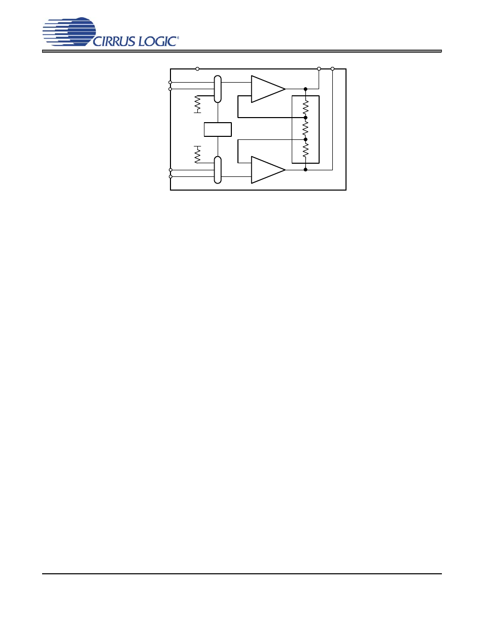
Page 16: 2 gain settings — gain, 2 amplifier outputs — outr, outf, 1 guard output — guard, Figure 13. cs5374 amplifier block diagram, Cs5374
CS5374
CS5374
16
3.
AMPLIFIER OPERATION
The CS5374 high-impedance, low-noise CMOS
differential input, differential output amplifiers are
optimized for precision analog signals between DC
and 2 kHz. They have multiplexed inputs and pro-
grammable gains of 1x, 2x, 4x, 8x, 16x, 32x, and
64x. The performance of this amplifier makes it
ideal for low-frequency, high-dynamic-range ap-
plications requiring low distortion and minimal
power consumption.
3.1 Amplifier Inputs — INA, INB
The amplifier analog inputs are designed for high-
impedance differential hydrophone sensors and so
have very low input bias below 1 pA.
3.1.1 Multiplexer Settings — MUX
Input multiplexing simplifies system connections
by providing separate inputs for a sensor and test
DAC (INA, INB) as well as an internal termination
for noise tests. The multiplexer determines which
input is connected to the amplifier, and is set
through internal configuration registers accessed
through the SPI port, see the “SPI
mary” on page 34 for more information.
Although a mux selection is provided to enable the
INA and INB switches simultaneously, significant
current should not be driven through them in this
mode. The CS5374 mux switches will maintain
good linearity only with minimal signal current.
3.1.2 Gain Settings
—
GAIN
The CS5374 supports gain ranges of 1x, 2x, 4,x 8x,
16x, 32x, and 64x. Amplifier gain is selected using
internal configuration registers accessed through
the SPI port, see the “SPI
on page 34 for more information.
3.2 Amplifier Outputs — OUTR, OUTF
The amplifier analog outputs are externally sepa-
rated into rough / fine charge signals to connect
into the modulator inputs. Each differential output
requires two series resistors and a differential ca-
pacitor to create the modulator anti-alias RC filter.
3.2.1 Guard Output — GUARD
The GUARD pin outputs the common mode volt-
age of the selected analog signal input. It can be
used to drive the cable shield between a high-im-
pedance sensor and the amplifier inputs. Driving
the cable shield with the analog signal common
mode voltage minimizes leakage and improves sig-
nal integrity from high-impedance sensors.
The GUARD output is defined as the midpoint
voltage between the + and – halves of the currently
INA1+
INB1+
MUX1
INB1-
INA1-
GUARD1
+
-
-
+
40
0
Ω
40
0
Ω
GAIN1
OUT1+ OUT1-
Figure 13. CS5374 Amplifier Block Diagram