4 adccfg — 0x03, 5 pwrcfg — 0x04, 4 adccfg — 0x03 5.3.5 pwrcfg — 0x04 – Cirrus Logic CS5374 User Manual
Page 24: Cs5374, Spi write transactions, Spi read transactions
CS5374
CS5374
24
5.3.4 ADCCFG — 0x03
The ADCCFG register can disable modulator
OFST and enable HP mode. It also enables PWDN
mode for the channel 1 & 2 modulators.
Reset Condition : 0000_0000
Normal Operation : 0100_0000
Power Down Operation : 0011_0000
5.3.5 PWRCFG — 0x04
The PWRCFG register can vary bias currents for
the amplifier and modulator to minimize power
consumption.
Reset Condition : 0000_0000
Normal Operation : 1000_1111
Power Down Operation : 0000_0000
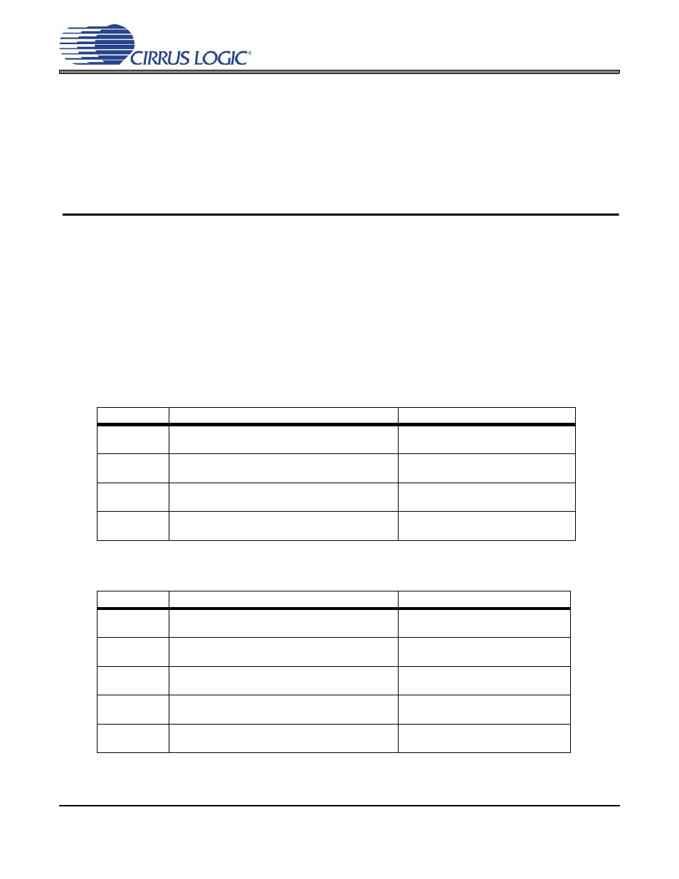
5.4 Example: CS5374 Configuration by an External SPI Master
Any SPI master that supports mode 0 (0,0) commu-
nication can write and read the configuration regis-
ters and control CS5374.
The following example SPI read and write transac-
tions show how to configure the CS5374 for nor-
mal operation.
SPI Write Transactions
Transaction
CS5374 SPI Write
Description
01
SI: 02 | 01 | 20
SO: -----------------
Write AMP1CFG register (0x01).
CH1 INA enabled, 1x gain (0x20).
02
SI: 02 | 02 | 20
SO: -----------------
Write AMP2CFG register (0x02).
CH2 INA enabled, 1x gain (0x20).
03
SI: 02 | 03 | 40
SO: -----------------
Write ADCCFG register (0x03).
Normal operation (0x40).
04
SI: 02 | 04 | 8F
SO: -----------------
Write PWRCFG register (0x04).
Normal operation (0x8F).
SPI Read Transactions
Transaction
CS5374 SPI Read
Description
01
SI: 03 | 00 | 00
SO: ---------- | 41
Read VERSION register (0x00).
Returned data byte on the SO pin.
02
SI: 03 | 01 | 00
SO: ---------- | 20
Read AMP1CFG register (0x01).
Returned data byte on the SO pin.
03
SI: 03 | 02 | 00
SO: ---------- | 20
Read AMP2CFG register (0x02).
Returned data byte on the SO pin.
04
SI: 03 | 03 | 00
SO: ---------- | 40
Read ADCCFG register (0x03).
Returned data byte on the SO pin.
05
SI: 03 | 04 | 00
SO: ---------- | 8F
Read PWRCFG register (0x04).
Returned data byte on the SO pin.
Table 4. Example SPI Transactions to Write and Read the CS5374 Configuration Registers