7 system signals – Cirrus Logic CS1810xx User Manual
Page 15
CobraNet Hardware User’s Manual
Pinout and Signal Descriptions
DS651UM23
©
Copyright 2005 Cirrus Logic, Inc.
15
Version 2.3
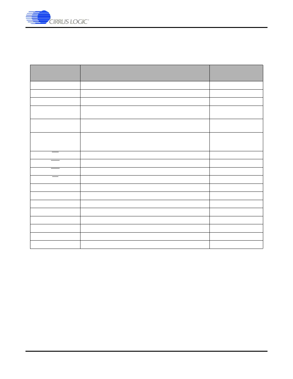
4.2.7 System Signals
Use these CS1810xx/CS4961xx signals stricktly in the manner described in
Schematics (Section 9.2 on page 44). Each signal is briefly described below.
Signal
Description
CS1810xx/CS4961xx
Pin #
VCXO_CTRL
A Delta-sigma DAC Output for Controlling the On-board VCXO
1
MCLK_SEL
Control Signal for Selecting MCLK Sources
2
DBDA, DBCK
I2C Debugger Interface
3, 4
TEST
Used for testing during manufacturing. Keep grounded for normal
operation.
9
DATA[15:0]
Data Bus for Flash & Ethernet Controller(s)
29-32, 34, 35, 37, 39-43,
45, 46, 48, 49
ADDR[19:0]
Address Bus for Flash & Ethernet Controller(s)
55, 56, 58, 59, 61, 62, 64,
67, 68, 70-72, 74, 75, 77,
82, 84, 85, 87, 88
WE
Write Enable for Flash and Ethernet Controller(s)
38
CS1
Chip Select for Flash Memory Device
90
CS2
Chip Select for Ethernet Controller(s)
65
OE
Output Enable
89
IOWAIT
Wait State Signal from Ethernet Controller(s)
96
GPIO[2:0]
General-purpose I/O Signals
99, 100, 108
XTI
Reference Clock Input / Crystal Oscillator Input
125
XTO
Crystal Oscillator Output
124
XTAL_OUT
A Buffered Version of XTI
123
FILT2, FILT1
PLL Loop Filter
127, 128
DAO_MCLK
MCLK Input
8
HS[3:0]
CS1810xx/CS4961xx Boot Mode Selection
11, 16, 17, 19