Car2512te front-end, Preliminary data sheet, Input: 90v – GE Industrial Solutions CAR2512TE Front-End User Manual
Page 10: Output: 12 v, Standby @ 15w, Pmbus, Command set, Status register bit allocation
GE
Preliminary Data Sheet
CAR2512TE Front-End
Input: 90V
AC
to 264V
AC
; Output: 12 V
DC
@ 2500W; 3.3/5V
DC
standby @ 15W
February 7, 2014
©2013 General Electric Company. All rights reserved.
Page 10
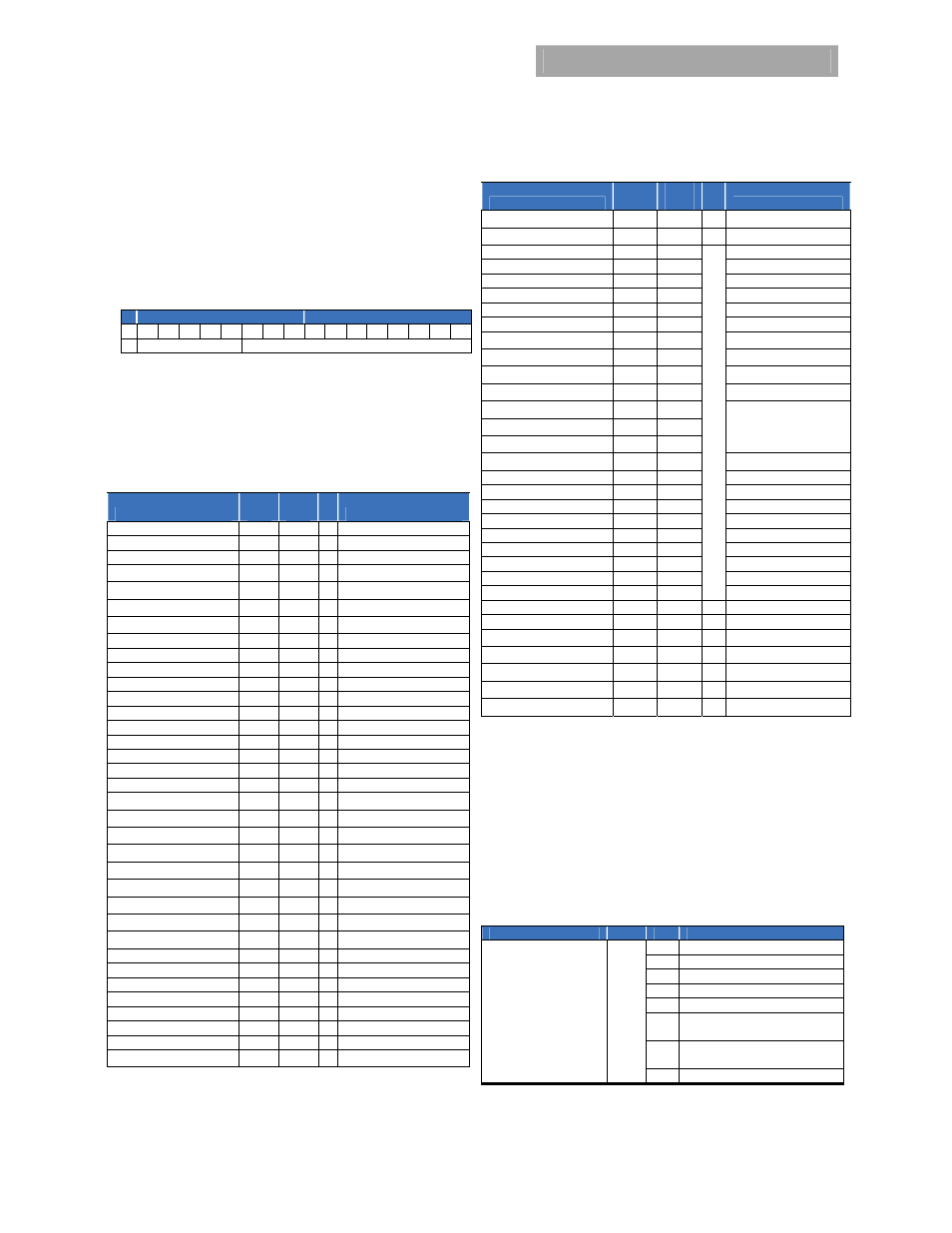
Linear Data Format
The definition is identical to Part II of the
PMBus Specification. All standard PMBus values, with the
exception of output voltage related functions, are represented
by the linear format described below. Output voltage functions
are represented by a 16 bit mantissa. Output voltage has a E=9
constant exponent.
The Linear Data Format is a two byte value with an 11-bit,
two’s complement mantissa and a 5-bit, two’s complement
exponent or scaling factor, its format is shown below.
Data Byte High
Data Byte Low
Bit 7 6 5 4 3 2 1 0 7 6 5 4 3 2 1 0
Exponent
(E)
Mantissa
(M)
The relationship between the Mantissa, Exponent, and Actual
Value (V) is given by the following equation:
E
M
V
2
Where: V is the value, M is the 11-bit, two’s omplement
mantissa, E is the 5-bit, two’s complement exponent
PMBus
TM
Command set:
Command
Hex
Code
Data
Byte
Function
Operation 01
1
W
Output
ON/OFF
ON_OFF_config
02
1
R Set at 1D, can’t change
Clear_faults 03
0
Clear
Status
Write_protect 10
1
W
Write
control
Store_default_all 11
0
W
Store
permanently
Restore_default_all 12 0
R
Reset
defaults
Capability
19
1
R 30h, 400kHz, SMBAlert
Vout_mode 20
1
R
Vout
constants
Vout_command 21
2
W
Set
Vout
Fan_command_1
3B
2
W Set fan speed in RPM
Vout_OV_fault_limit
40
2
W Set OV fault limit
Vout_OV_fault_response 41 1 W
Vout_OV_warn_limit
42
2
W Set OV warn limit
Vout_UV_warn_limit
43
2
W Set UV warn limit
Vout_UV_fault_limit 44
2
W
Vout_UV_fault_response 45 1 W
Iout_OC_fault_limit 46
2
W
Iout_OC_fault_response
47 1
W Latch or hiccup
Iout_OC_warn_limit 4A
2
W Set OC warn limit
OT_fault_limit 4F
2
W
OT_fault_response 50
1
W Latch or hiccup
OT_warn_limit 51
2
W Set OT warn limit
Vin_OV_fault_limit 55
2
W
Vin_OV_warn_limit 57
2
W Set OV warn limit
Vin_UV_warn_limit
58
2
W Set UV warn limit
Vin_UV_fault_limit
59
2
W Set UV shutdown
Status_byte 78
1
R
Status_word 79
2
R
Status_Vout 7A
1
R
Status_Iout 7B
1
R
Status_input 7C
1
R
Status_temperature 7D
1
R
Status_CML 7E
1
R
Status_other 7F
1
R
Command
Hex
Code
Data
Field
Function
Status_mfr_specific
80 1
R
Status_fan_1_2
81 1
R
Read_Vin 88
2
R
Read input voltage
Read Iin
89
2
Read input current
Read_Vout 8B
2
Read
output
voltage
Read_Iout 8C
2
Read
output
current
Read_temperature 8D
2 Read
Temperature
Read_fan_speed_1 90
2 In
RPM
Read_fan_speed_2
91 2
In
RPM
Read_Pout 96
2
Read_Pin
97 2
PMBus revision
98
1
Mfr_ID 99
5
FRU_ID
Mfr_model 9A
16
Mfr_serial 9E
15
Mfr_Vin_min A0
2
Mfr_Vin_max A1
2
Mfr_Iin_max A2
2
Mfr_Pin_max A3
2
Mfr_Vout_min A4
2
Mfr_Vout_max A5
2
Mfr_Iout_max A6
2
Mfr_Pout_max A7
2
Mfr_Tambient_max A8
2
Mfr_Tambient_min A9
2
User_data_00
B0
48
W User memory space
User_data_01
B1
48
W User memory space
Read_mfr_revision D5
4
R
Fan_duty_cycle
D6
1
W Duty_cycle in %
Fan_speed D7
1
W Control in duty cycle
Vprog_ext D8
2
W
Notes:
Settings and read backs above support the 12Vdc main
output. There are no adjustments or read backs of the standby
output. Failure of the standby output is reported by the
STATUS_MFR_SPECIFIC register. The code does not check the
validity of, or whether the data being changed is within the
expected boundary. The user is responsible to make sure that
data placed in the registers is within the monitored range.
Status Register Bit Allocation:
Register
Code Bit
Function
Status_Byte 78
7 Busy
6 DC_
OFF
5
Output OV Fault detected
4
Output OC Fault detected
3
Input UV Fault detected
2 Temperature
Fault/warning
detected
1 CML
(communication
fault)
detected
0
None of Below