Pin description detailed description – Rainbow Electronics MAX3745 User Manual
Page 6
MAX3744/MAX3745
2.7Gbps SFP Transimpedance
Amplifiers with RSSI
6
_______________________________________________________________________________________
Pin Description
Detailed Description
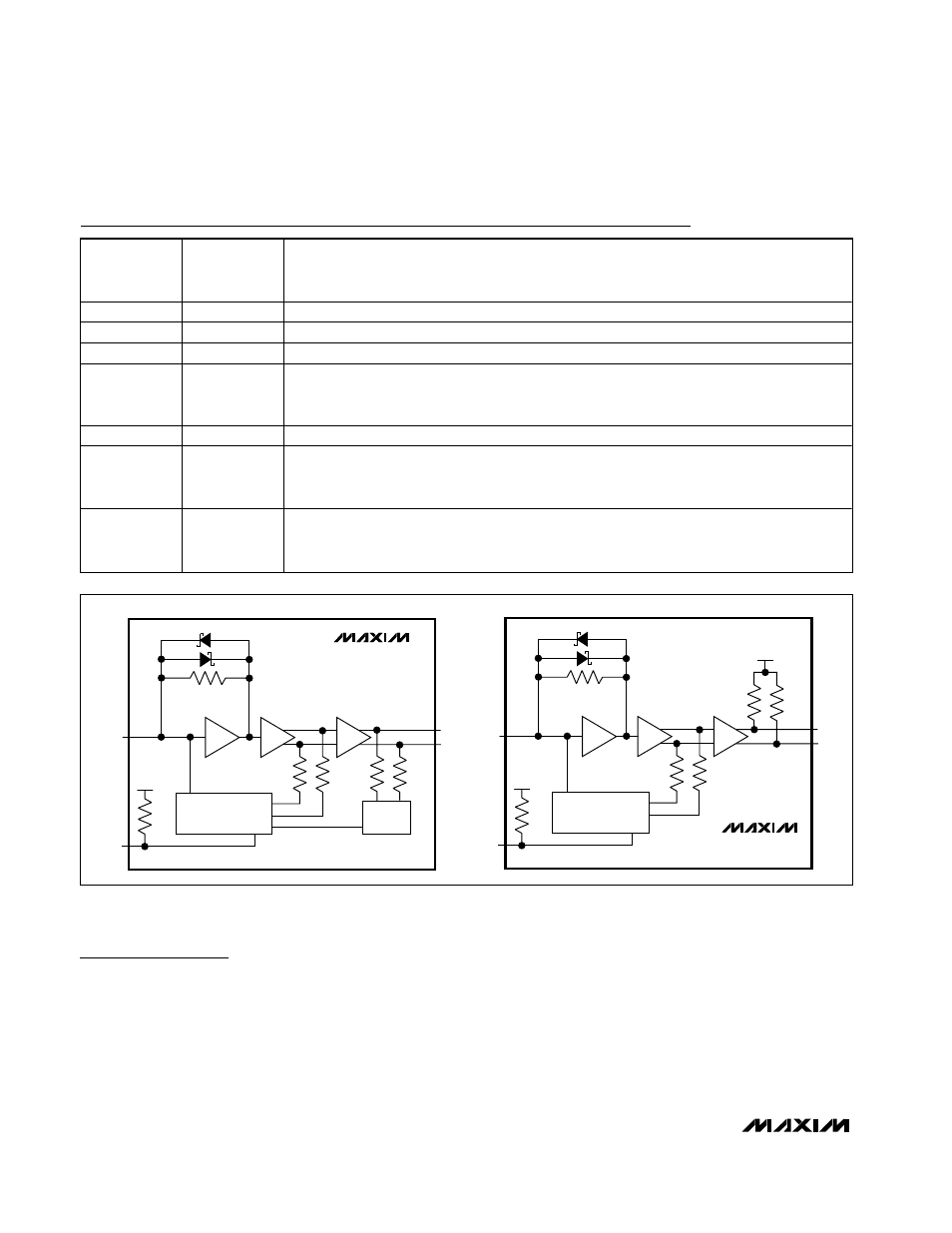
The MAX3744/MAX3745 are transimpedance amplifiers
designed for up to 2.7Gbps SFF/SFP transceiver mod-
ules. A functional diagram of the MAX3744/MAX3745 is
shown in Figure 1. The MAX3744/MAX3745 comprise a
transimpedance amplifier stage, a voltage amplifier
stage, an output buffer, and a direct-current (DC) feed-
back cancellation circuit. The MAX3744 also includes a
signal strength indicator (RSSI). To provide this signal in
a standard 4-pin TO header, the RSSI level is added to
the common mode of the differential data output pins.
Transimpedance Amplifier Stage
The signal current at the input flows into the summing
node of a high-gain amplifier. Shunt feedback through
the resistor R
F
converts this current to a voltage. In par-
allel with the feedback resistor are two back-to-back
Schottky diodes that clamp the output signal for large
input currents, as shown in Figure 2.
MAX3744/
MAX3745
BOND PAD
NAME
FUNCTION
1, 3
V
CC
Supply Voltage
2, 7
N.C.
No Connection
4
IN
TIA Input. Signal current from photodiode flows into this pin.
5
FILTER
Provides bias voltage for the photodiode through a 580
Ω resistor to V
CC
. When grounded, this
pin disables the DC cancellation amplifier to allow a DC path from IN to OUT+ and OUT- for
testing.
6, 10
GND
Supply Ground
8
OUT-
Inverting Data Output. Current flowing into IN causes the voltage at OUT- to decrease. For the
MAX3744, the common mode between OUT+ and OUT- is proportional to the average input
current.
9
OUT+
Noninverting Data Output. Current flowing into IN causes the voltage at OUT+ to increase. For
the MAX3744, the common mode between OUT+ and OUT- is proportional to the average input
current.
TRANSIMPEDANCE
AMPLIFIER
OUT+
50
Ω
50
Ω
OUT-
V
CC
FILTER
IN
DC CANCELLATION
CIRCUIT
MAX3744
RSSI
TRANSIMPEDANCE
AMPLIFIER
OUT+
50
Ω
50
Ω
OUT-
V
CC
FILTER
IN
DC CANCELLATION
CIRCUIT
MAX3745
V
CC
R
F
R
F
Figure 1. Functional Diagram