Rainbow Electronics MAX3745 User Manual
Page 2
MAX3744/MAX3745
2.7Gbps SFP Transimpedance
Amplifiers with RSSI
2
_______________________________________________________________________________________
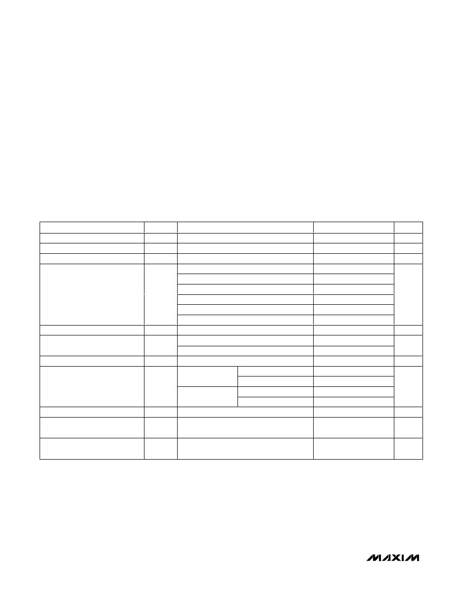
ABSOLUTE MAXIMUM RATINGS
ELECTRICAL CHARACTERISTICS
(V
CC
= +2.97V to +3.63V and T
A
= -40°C to +85°C. Typical values are at V
CC
= +3.3V, source capacitance (C
IN
) = 0.85pF, and T
A
=
+25°C, unless otherwise noted.) (Notes 1, 2)
Stresses beyond those listed under “Absolute Maximum Ratings” may cause permanent damage to the device. These are stress ratings only, and functional
operation of the device at these or any other conditions beyond those indicated in the operational sections of the specifications is not implied. Exposure to
absolute maximum rating conditions for extended periods may affect device reliability.
Power-Supply Voltage (V
CC
) .................................-0.5V to +6.0V
Continuous CML Output Current
(OUT+, OUT-) ............................................. -25mA to +25mA
Continuous Input Current (IN)...............................-4mA to +4mA
Continuous Input Current (FILTER).......................-8mA to +8mA
Operating Junction Temperature Range (T
J
) ....-55°C to +150°C
Storage Ambient Temperature Range (T
STG
) ...-55°C to +150°C
Die Attach Temperature...................................................+400°C
PARAMETER
SYMBOL
CONDITIONS
MIN
TYP
MAX
UNITS
Supply Current
I
CC
Including CML output current (I
IN
= 0)
28
41
mA
Input Bias Voltage
1.0
V
Input Overload
(Note 3)
2
mA
P-P
C
IN
= 0.85pF, BW = 933MHz
206
C
IN
= 0.85pF, BW = 2.1GHz
330
430
C
IN
= 0.85pF, BW = 18GHz
620
C
IN
= 0.6pF, BW = 933MHz
206
C
IN
= 0.6pF, BW = 2.1GHz
300
380
Input-Referred Noise
I
N
C
IN
= 0.6pF, BW = 18GHz
550
nA
RMS
Differential Transimpedance
Differential output, I
IN
= 40µA
AVE
2.8
3.5
4.5
k
Ω
-3dB, C
IN
= 0.6pF
1.8
2
Small-Signal Bandwidth (Note 3)
BW
-3dB, C
IN
= 0.85pF
1.6
1.8
GHz
Low-Frequency Cutoff
-3dB, input current = 20µA
AVE
(Note 3)
30
kHz
2.1Gbps, K28.5 pattern
14
31
100µA
P-P
< input
≤
2mA
P-P
2.7Gbps, 2
31
-1 pattern
24
2.1Gbps, K28.5 pattern
10
16
Deterministic Jitter
(Notes 3, 5)
DJ
10µA
P-P
< input
≤
100µA
P-P
2.7Gbps, 2
31
-1 pattern
20
ps
P-P
Filter Resistance
510
580
690
Ω
Differential Output Resistance
(OUT+, OUT-)
85
100
115
Ω
Maximum Differential Output
Voltage
V
OD
Input > 50µA
AVE
, output termination 50
Ω to
V
CC
(output in limited state)
220
280
400
mV
P-P