Electrical characteristics (continued) – Rainbow Electronics MAX3745 User Manual
Page 3
MAX3744/MAX3745
2.7Gbps SFP Transimpedance
Amplifiers with RSSI
_______________________________________________________________________________________
3
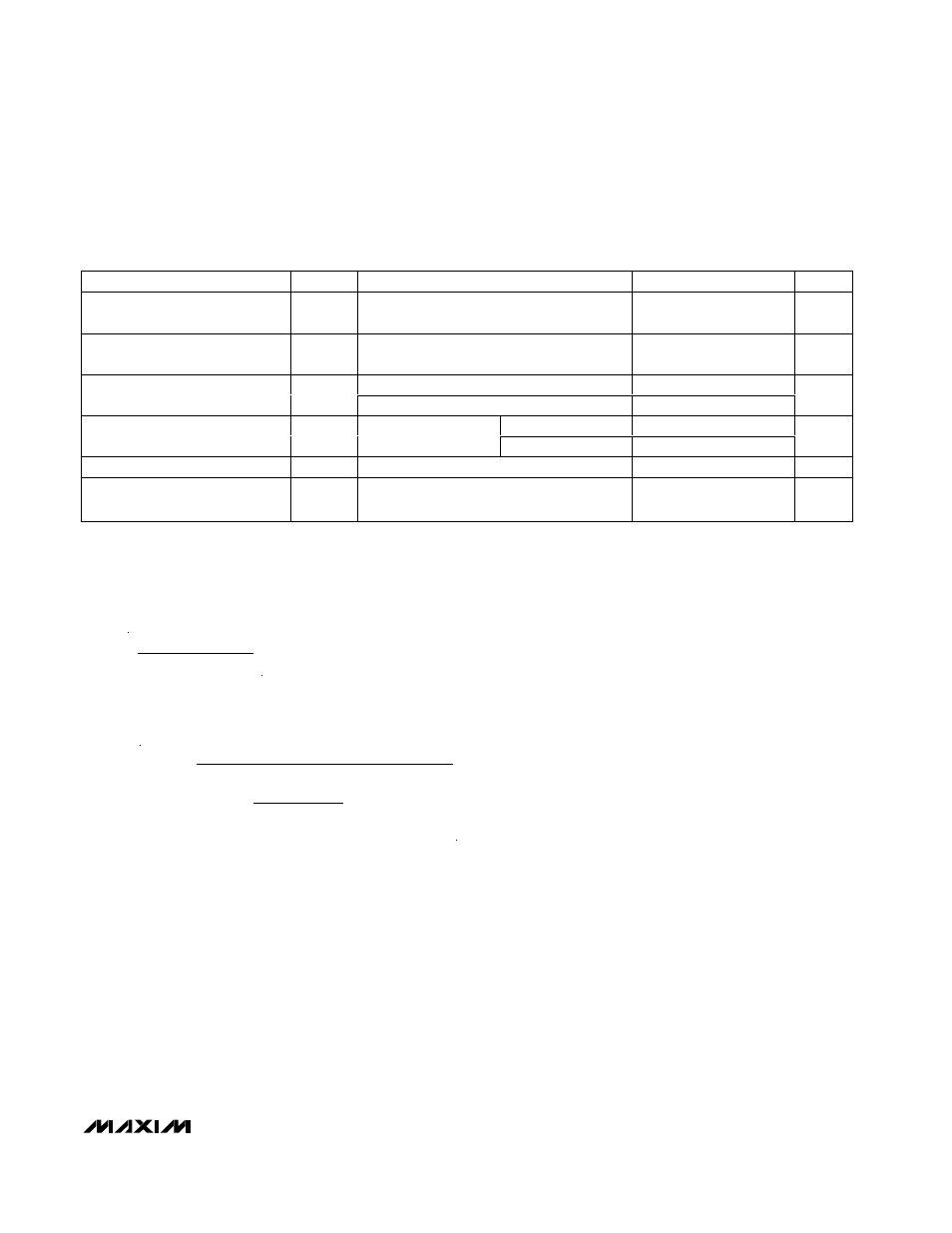
ELECTRICAL CHARACTERISTICS (continued)
(V
CC
= +2.97V to +3.63V and T
A
= -40°C to +85°C. Typical values are at V
CC
= +3.3V, source capacitance (C
IN
) = 0.85pF, and T
A
=
+25°C, unless otherwise noted.) (Notes 1, 2)
Note 1: Die parameters are production tested at room temperature only, but are guaranteed by design and characterization from
-40
°C to +85°C.
Note 2: Source capacitance represents the total capacitance at the IN pad during characterization of the noise and bandwidth para-
meters.
Note 3: Guaranteed by design and characterization.
Note 4: Input-referred noise is:
Note 5: Deterministic jitter is the sum of pulse-width distortion (PWD) and pattern-dependent jitter (PDJ).
Note 6: Power-supply noise rejection PSNR = -20log(
∆V
OUT
/
∆V
CC
), where
∆V
OUT
is the differential output voltage and
∆V
CC
is the
noise on V
CC
.
Note 7:
A
I
I
A
I
I
A
A
where I
I
I
RSSI range is from I
A to
A
RSSI
OUT CM IN
OUT CM IN
OUT CM
OUT
OUT
IN
=
=
−
=
=
+
=
+
−
_
_
_
(
)
(
)
400
0
400
2
6
500
µ
µ
µ
µ
µ
RMS output noise
Gain at f
MHz
=
100
PARAMETER
SYMBOL
CONDITIONS
MIN
TYP
MAX
UNITS
Single-Ended Output Common-
Mode Minimum Level (MAX3744)
Relative to V
CC
, I
IN
= 1mA
AVE
540
490
mV
Output Data Transition Time
Input > 200µA
P-P
20% to 80% rise/fall time
(Note 3)
80
140
ps
Frequency
≤ 1GHz
17
Differential Output Return Loss
1GHz < frequency
≤ 2GHz
10
TBD
f < 1MHz
46
Power-Supply Noise Rejection
PSNR
I
IN
= 0
(Note 6)
1MHz
≤ f < 10MHz
34
dB
RSSI Gain (MAX3744)
A
RSSI
(Note 7)
21
A/A
RSSI Gain Stability (MAX3744)
10log(A
RSSI
/A
RSSI-NOM
) where A
RSSI-NOM
=
A
RSSI
at 3.3V, +25°C (Note 3)
0.24
dB