Detailed description and applications information, Pin description – Rainbow Electronics MAX3805 User Manual
Page 5
Detailed Description and
Applications Information
The MAX3805 adaptive equalizer is designed to oper-
ate with 9.95Gbps to 10.7Gbps PRBS nonreturn-to-zero
(NRZ) data at the receive end of a transmission line,
typically differential 6-mil FR-4 PC board. It adaptively
corrects intersymbol interference caused by frequency-
dependent path loss. It can also be used with coaxial
cable links and with transmission lines that include well-
engineered connectors, as long as the total path loss is
relatively smooth and does not exceed 20dB at 5GHz.
The signal path for the MAX3805 consists of a CML
input stage, two amplifiers feeding a pair of variable
attenuators controlled by feedback, and a limiting
amplifier with a CML output stage. An enable input, EN,
is used to control the output stage. A signal-detect out-
put, SD, indicates when input signal to the transmission
line is above 220mV
P-P
or below 200mV
P-P
, typically.
See the Functional Diagram.
CML Input and Output Buffers
The MAX3805 CML input and output buffers are inter-
nally terminated with 50
Ω to V
CC1
and V
CC2
, respec-
tively. The input and output circuitry have separate
voltage connections to control noise coupling and pro-
vide DC-coupling to +1.8V, +2.5V, or +3.3V CML. If
desired, the CML inputs and outputs can be AC-cou-
pled. See Figure 1 for the output structure.
The low-frequency cutoff of the input-stage offset-can-
cellation circuit is nominally 21kHz.
For single-ended operation (typically coaxial cable
links), the input must be AC-coupled; connect the
unused input to V
CC1
using a series combination of an
AC-coupling capacitor and a 50
Ω resistor, as shown in
Figure 2. Note that the MAX3805 is specified for differ-
ential operation, and the performance may be reduced
in single-ended operation.
MAX3805
10.7Gbps Adaptive Receive Equalizer
_______________________________________________________________________________________
5
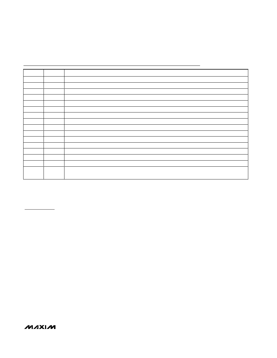
Pin Description
PIN
NAME
FUNCTION
1
V
CC1
Supply Voltage, CML Input (1.8V to V
CC
)
2
SDI+
Positive Differential Serial Data Input, CML
3
SDI-
Negative Differential Serial Data Input, CML
4
V
CC1
Supply Voltage, CML Input (1.8V to V
CC
)
5
GND
Supply Ground
6
SD
Signal-Detect Output, LVCMOS. Low indicates <200mV
P-P
, high indicates >220mV
P-P
.
7
EN
Enable Input, LVCMOS. Low disables output, high enables output, typically connected to SD.
8
GND
Supply Ground
9, 12
V
CC2
Supply Voltage, CML Output (1.8V to V
CC
)
10
SDO-
Negative Differential Serial Data Output, CML
11
SDO+
Positive Differential Serial Data Output, CML
13
HFPD
High-Frequency Power Detector. Leave open for 9.953Gbps to 10.7Gbps PRBS NRZ data.
14
LFPD
Low-Frequency Power Detector. Leave open for 9.953Gbps to 10.7Gbps PRBS NRZ data.
15
V
CC
Supply Voltage, Equalizer Core, 3.3V
16
GND
Supply Ground
EP
Exposed
Pad
Ground. The exposed pad must be soldered to the circuit board ground plane for proper thermal and
electrical performance.