Operating conditions – Rainbow Electronics MAX3805 User Manual
Page 2
MAX3805
10.7Gbps Adaptive Receive Equalizer
2
_______________________________________________________________________________________
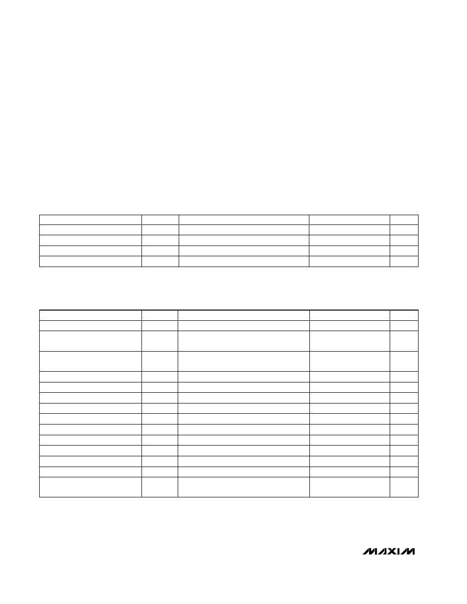
ABSOLUTE MAXIMUM RATINGS
ELECTRICAL CHARACTERISTICS
(Pin 13 (HFPD) and pin 14 (LFPD) are not connected. Typical values are at V
CC
= +3.3V, V
CC1
= V
CC2
= 1.8V, T
A
= +25
°C, unless
otherwise noted.) (Values at -40°C are guaranteed by design and characterization.)
Stresses beyond those listed under “Absolute Maximum Ratings” may cause permanent damage to the device. These are stress ratings only, and functional
operation of the device at these or any other conditions beyond those indicated in the operational sections of the specifications is not implied. Exposure to
absolute maximum rating conditions for extended periods may affect device reliability.
Supply Voltage (V
CC
) ............................................-0.5V to +4.0V
CML Supply Voltage
(V
CC1
, V
CC2
) ..........................................-0.5V to (V
CC
+ 0.5V)
Current at SDO±...............................................................±25mA
SDI±, EN, SD, HFPD, LFPD........................-0.5V to (V
CC
+ 0.5V)
Current at HFPD, LFPD ......................................................400µA
Continuous Power Dissipation (T
A
= +85°C)
16-Lead QFN-EP (derate 17.5mW/°C
above +85°C) ............................................................1398mW
Operating Ambient Temperature Range .............-40°C to +85°C
Storage Ambient Temperature Range...............-55°C to +150°C
Lead Temperature (soldering, 10s) .................................+300°C
PARAMETER
SYMBOL
CONDITIONS
MIN
TYP
MAX
UNITS
Supply Current
I
CC
V
CC
= V
CC1
= V
CC2
41
60
mA
CML Input Differential Voltage
V
IN
AC-coupled or DC-coupled at transmission
line input (Notes 1, 6)
400
1200
mV
P-P
CML Input Common-Mode
Voltage
1.3
V
CC1
V
CML Input Resistance
Differential
85
100
115
Ω
CML Input Return Loss
100MHz to 10GHz
10
dB
CML Output Differential Voltage
V
OUT
V
CC2
= 1.65V to 3.6V
400
500
600
mV
P-P
CML Output Resistance
Differential
85
100
115
Ω
CML Output Transition Time
t
r
/t
f
20% to 80% (Notes 2, 6)
35
ps
CML Output Return Loss
100MHz to 5GHz
10
dB
Equalizer Time Constant
10
µs
Output Residual Jitter
(Notes 3–6)
21
30
ps
P-P
Signal-Detect Assert
PRBS2
31
- 1 at 10.7Gbps (Note 1)
200
mV
P-P
Signal-Detect Deassert
PRBS2
31
- 1 at 10.7Gbps (Note 1)
220
mV
P-P
LVCMOS Input-High Leakage
Current
I
H
+10
+60
µA
PARAMETER
SYMBOL
CONDITIONS
MIN
TYP
MAX
UNITS
Supply Voltage
V
CC
3.0
3.3
3.6
V
Input Termination Voltage
V
CC1
1.65
V
CC
V
Output Termination Voltage
V
CC2
1.65
V
CC
V
Operating Ambient Temperature
-40
+25
+85
°C
OPERATING CONDITIONS