Absolute maximum ratings, Electrical characteristics – Rainbow Electronics MAX3795 User Manual
Page 2
MAX3795
1Gbps to 4.25Gbps Multirate VCSEL Driver
with Diagnostic Monitors
2
_______________________________________________________________________________________
ABSOLUTE MAXIMUM RATINGS
Stresses beyond those listed under “Absolute Maximum Ratings” may cause permanent damage to the device. These are stress ratings only, and functional
operation of the device at these or any other conditions beyond those indicated in the operational sections of the specifications is not implied. Exposure to
absolute maximum rating conditions for extended periods may affect device reliability.
Supply Voltage (V
CC
) ............................................-0.5V to +4.0V
Voltage at TX_DISABLE, IN+, IN-, FAULT,
SQUELCH, TC1, TC2, MODSET, PEAKSET, BIASSET,
BIAS, BIASMON, COMP, MD, REF,
PWRMON ...............................................-0.5V to (V
CC
+ 0.5V)
Voltage at OUT+, OUT- .........................(V
CC
- 2V) to (V
CC
+ 1V)
Current into FAULT ............................................ -1mA to +25mA
Current into OUT+, OUT- ....................................................60mA
Continuous Power Dissipation (T
A
= +85°C)
24-Pin Thin QFN
(derate 20.8mW/°C above +85°C).................................1354mW
Storage Temperature Range .............................-55°C to +150°C
Lead Temperature (soldering, 10s) .................................+300°C
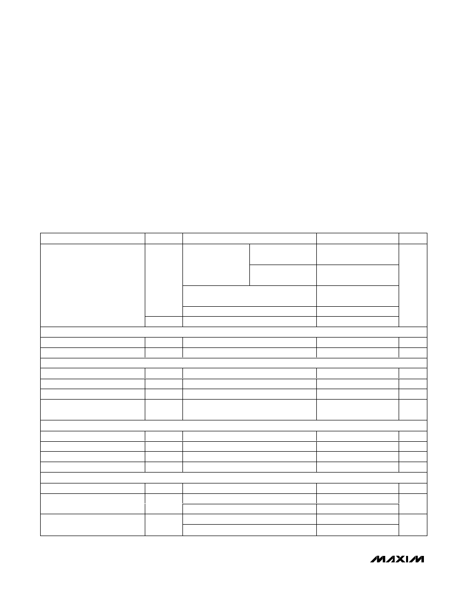
ELECTRICAL CHARACTERISTICS
(V
CC
= +2.97V to +3.63V, T
A
= -40°C to +85°C. Typical values are at V
CC
= +3.3V, TC1 and TC2 are shorted, PEAKSET open, T
A
=
+25°C, unless otherwise noted.)
PARAMETER
SYMBOL
CONDITIONS
MIN
TYP
MAX
UNITS
I
MOD
= 2mA
P-P
35
SQUELCH set low,
TX_DISABLE set low,
peaking is not used
(Note 1)
I
MOD
= 15mA
P-P
71
81
Additional current when peaking is used,
R
PEAK
= 1.18k
Ω
15
I
CC
Additional current when SQUELCH is high
5
10
Supply Current
I
CC-SHDN
Total current when TX_DISABLE is high
7
mA
FAULT OUTPUT
Output High Voltage
V
OH
R
LOAD
= 10k
Ω to 2.97V
2.4
V
Output Low Voltage
V
OL
R
LOAD
= 4.7k
Ω to 3.63V
0.4
V
TX_DISABLE INPUT
Input Impedance
R
PULL
4.7
8
10.0
k
Ω
Input High Voltage
V
IH
2.0
V
Input Low Voltage
V
IL
0.8
V
Power-Down Time
The time for I
CC
to reach I
CC-SHDN
when
TX_DISABLE transitions high
50
µs
SQUELCH
Squelch Threshold
25
85
mV
P-P
Squelch Hysteresis
6
mV
P-P
Time to Squelch Data
(Note 3)
0.02
5.00
µs
Time to Resume from Squelch
(Note 3)
0.02
5.00
µs
BIAS GENERATOR
Maximum Bias Pin Voltage
V
BIAS-MAX
Referenced to V
CC
-0.65
V
Minimum
1
Bias Current
I
BIAS
Maximum
15
mA
5mA
≤ I
BIAS
≤ 15mA
-8
+8
Accuracy of Programmed Bias
Current
∆BIAS
1mA
≤ I
BIAS
≤ 5mA
-12
+12
%