Electrical characteristics (continued) – Rainbow Electronics MAX1464 User Manual
Page 7
MAX1464
Low-Power, Low-Noise Multichannel
Sensor Signal Processor
_______________________________________________________________________________________
7
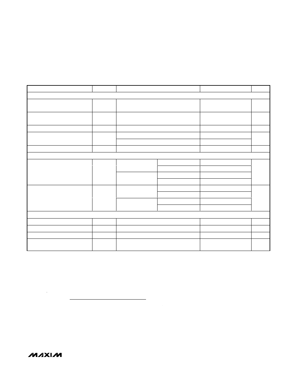
PARAMETER
SYMBOL
CONDITIONS
MIN
TYP
MAX
UNITS
DIGITAL INPUTS (GPIO1, GPIO2, SCLK, DI, CKSEL, CKIO, CS)
Input High Threshold Voltage
V
IH
0.8 x
V
DD
V
Input Low Threshold Voltage
V
IL
0.2 x
V
DD
V
Input Hysteresis
V
IHYS
0.2
V
CKSEL, CS = V
SS
38
-90
Input Leakage Current
I
IN
GPIO1, GPIO2, SCLK, DI, CKIO = V
DD
38
+90
µA
Input Capacitance
C
IN
5
pF
DIGITAL OUTPUTS (GPIO1, GPIO2, DO, CKIO)
GPIO1, GPIO2, DO
V
DD
- 0.1
R
LOAD
=
∞
CKIO (Note 10)
4.9
GPIO1, GPIO2, DO
V
DD
- 0.15
Output-Voltage High
V
OH
R
LOAD
= 2k
Ω to V
SS
CKIO (Note 10)
4.6
V
GPIO1, GPIO2, DO
0.05
R
LOAD
=
∞
CKIO (Note 10)
0.1
GPIO1, GPIO2, DO
0.2
Output-Voltage Low
V
OL
R
LOAD
= 2k
Ω to V
DD
CKIO (Note 10)
0.4
V
FLASH MEMORY
Maximum Erase Cycles
(Notes 11, 12)
10k
Cycles
Minimum Erase Time
t
ERASE
(Notes 11, 12)
4.2
ms
Minimum Write Time
t
WRITE
(Notes 11, 12)
80
µs
FLASH Programming Current
I
DDFP
Writing to the FLASH or erasing the FLASH
(Note 13)
30
mA
ELECTRICAL CHARACTERISTICS (continued)
(V
DDF
= V
DD
= 4.5V to 5.5V, V
SSF
= V
SS
= 0V, f
CLK
= 4.0MHz, T
A
= T
MIN
to T
MAX
. Typical values are at V
DDF
= V
DD
= 5.0V, V
SSF
= V
SS
= 0V,
T
A
= +25°C, unless otherwise noted.) (Note 1)
Note 1:
Current into a pin is defined as positive. Current out of a pin is defined as negative. All voltages are referenced to V
SS
.
Note 2:
All modules are off, except internal reference, oscillator, and power-on reset (POR) and CKSEL bit is set to zero.
Note 3:
The CPU and ADC are not on at the same time. The ADC and CPU currents are not additive.
Note 4:
I
DACn
does not include output buffer currents (I
OPLGn
or I
OPSMn
).
Note 5:
For gains above 240, an additional digital gain can be provided by the CPU.
Note 6:
The PWM input data is the 12-bit left-justified data in the 16-bit input field.
Note 7:
PWM gain error measured as:
Note 8:
The internal reference voltage has a nominal value of 5V (4
✕
V
BG
) even when V
DD
is greater or less than 5VDC.
Note 9:
Input-referred offset error is the ADC offset error divided by the PGA gain.
Note 10: When the CKIO is configured in output mode to observe the internal oscillator signal, the total current is above the
specified limits.
Note 11: f
CLK
must be within 5% of 4MHz.
Note 12: Allow a minimum elapsed time of 4.2ms when executing a FLASH erase command, before sending any other command.
Allow a minimum elapsed time of 80µs between FLASH write commands.
Note 13: FLASH programming current is guaranteed by design.
GE
PWM
F
Xh
PWM
Xh
PWM
OUT
OUT
=
(
)
−
(
)
Ч
00
100
3584
100%