Rainbow Electronics MAX1464 User Manual
Page 20
MAX1464
Low-Power, Low-Noise Multichannel
Sensor Signal Processor
20
______________________________________________________________________________________
FLASH Memory
There are 4096 bytes of programmable/erasable FLASH
memory for CPU program instructions and coefficients
storage. In addition, there are 128 bytes of FLASH mem-
ory accessible only by the serial interface for storage of
user information data.
These two FLASH memory locations are separated as
partitions. The program/coefficient memory is FLASH
partition 0 and the information memory is FLASH parti-
tion 1. Each partition is accessible by the serial inter-
face for reading, erasing, and writing data. Program/
coefficient memory partition 0 is accessible by the CPU
as read only, and partition 1 is not accessible by the
CPU. The CPU cannot erase or write data to either of
the FLASH memory partitions.
FLASH partition 0 is selected during the POR cycle.
FLASH partition 1 is selected by sending the halt CPU
command (IRS[7:0] = 78h) and changing the partition
selected by sending the change partition command
(IRS[7:0] = F8h). A following halt command (IRS[7:0] =
78h) resets the selected partition to partition 0.
Modifying the FLASH Contents
The MAX1464 FLASH memory contents must be erased
(contents = FFh) before the desired contents can be writ-
ten. There is no individual byte-erase command, but
either a total-erase command (IRS[7:0] = E8h) where all
the selected partition is erased (4kB for partition 0 or 128
bytes for partition 1) or a page-erase command (IRS[7:0]
= D8h), where only 64 bytes are erased, and the page is
selected by PFAR[11:6]. There are 64 pages in FLASH
partition 0, and only 2 pages in FLASH partition 1.
The programming of the MAX1464 FLASH memory
must use the following procedure (all the commands
are to be sent through the serial interface, and are
hexadecimal values of IRS[7:0]):
IRS0
IRSA0
IRS1
IRSA1
IRS2
IRSA2
IRS3
IRSA3
IRS4
IRSD0
IRS5
IRSD1
IRS6
IRSD2
IRS7
IRSD3
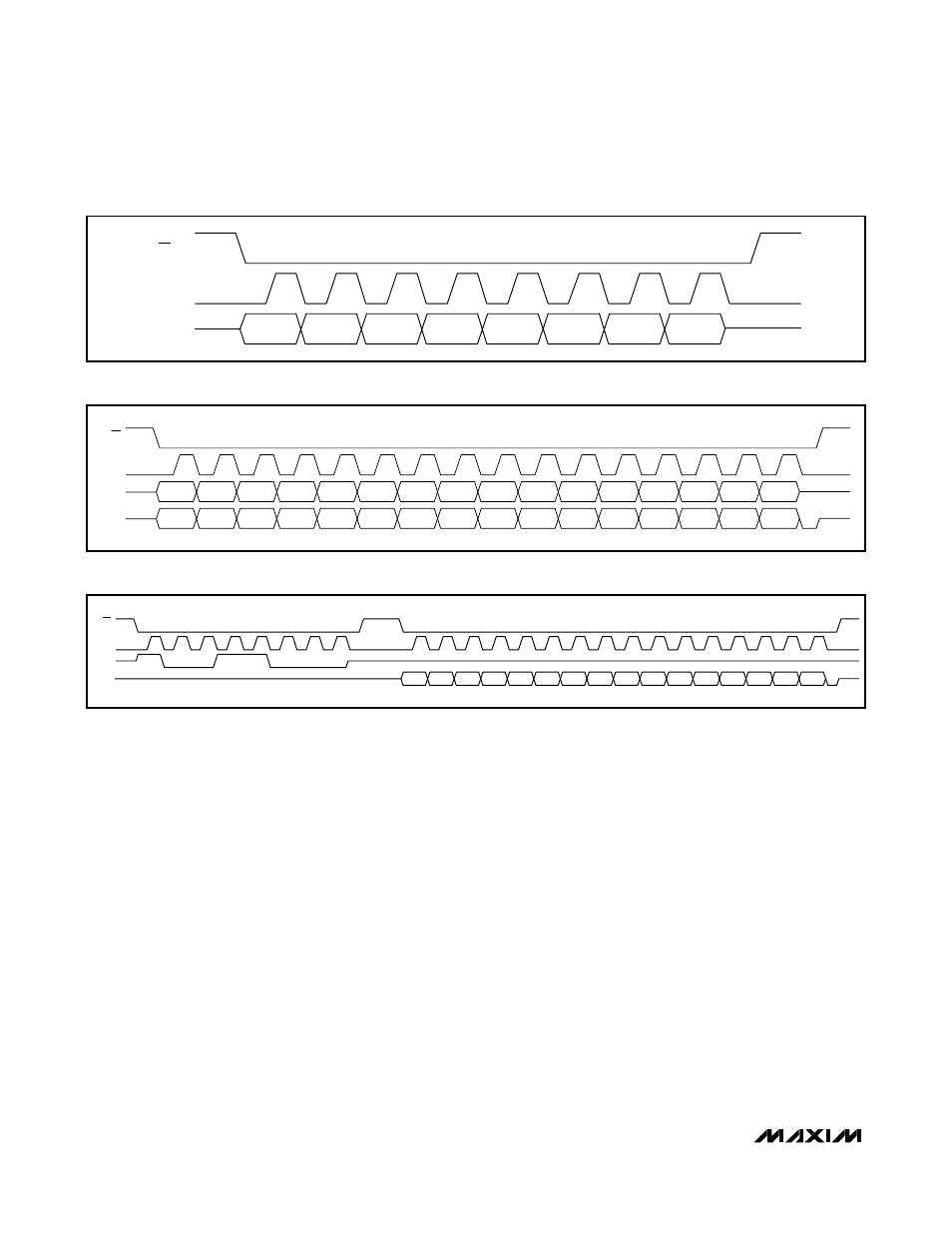
SCLK
DI
CS
Figure 8. Serial Interface Data Input
IRS0
IRSA0
IRS2
IRSA2
IRS3
IRSA3
IRS4
IRSD0
IRS5
IRSD1
IRS6
IRSD2
IRS7
IRSD3
IRS0
IRSA0
IRS1
IRSA1
IRS2
IRSA2
IRS3
IRSA3
IRS4
IRSD0
IRS5
IRSD1
IRS6
IRSD2
IRS7
IRSD3
DHR15
DHR14
DHR13
DHR12
DHR11
DHR10
DHR9
DHR8
DHR7
DHR6
DHR5
DHR4
DHR3
DHR2
DHR1
DHR0
CS
SCLK
DI
DO
IRS1
IRSA1
Figure 9. 4-Wire Mode Data Read from DHR Register
DHR15 DHR14 DHR13 DHR12 DHR11 DHR10 DHR9 DHR8 DHR7 DHR6 DHR5 DHR4 DHR3 DHR2 DHR1 DHR0
1
IRSA0
0
IRSA1
0
IRSA2
1
IRSA3
1
IRSD0
0
IRSD1
0
IRSD2
0
IRSD3
CS
SCLK
DI
DO
Figure 10. 3-Wire Mode Data Read from DHR Register