Rainbow Electronics MAX1464 User Manual
Page 15
MAX1464
Low-Power, Low-Noise Multichannel
Sensor Signal Processor
______________________________________________________________________________________
15
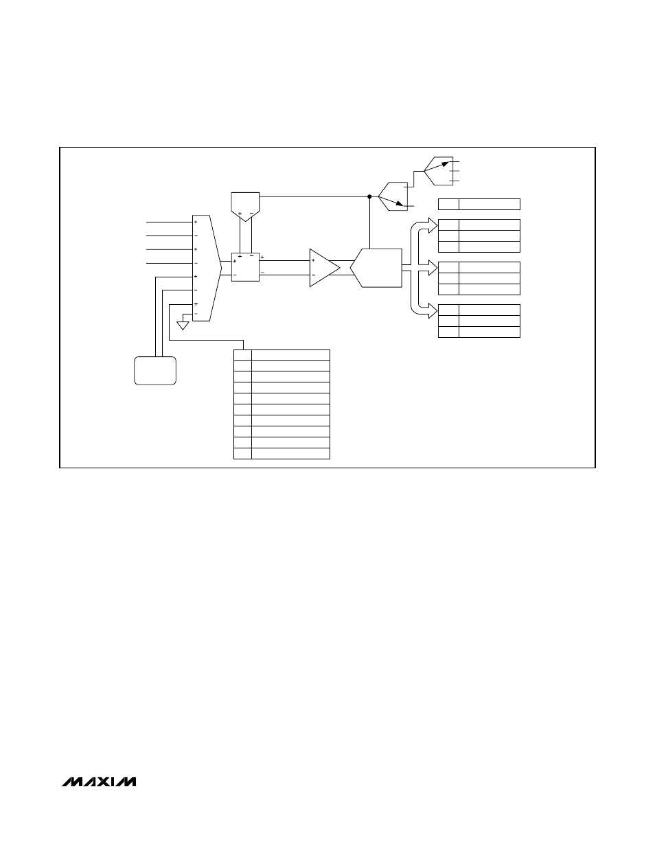
Single-ended inputs can be converted by either channel
1 or 2 by initiating a conversion on the appropriate chan-
nel with the SE[3:0] bits set to the desired single-ended
input (Table 7). Several of the single-ended signals are
converted with a fixed gain. The reduced gain of 0.7V/V
allows signals at or near the supply rails to be converted
without concern of saturation. Other single-ended signals
can be converted with the full selectable PGA gain range.
Programmable-Gain Amplifier
The gain of the differential inputs and several
single-ended inputs can be set to values between
0.99V/V to 244V/V as shown in Table 14. The PGA bits
are set in ADC_Config_nA where n = 1, 2, or T. The gain
setting must be selected prior to initiating a conversion.
ADC Conversion Time and Resolution
The ADC conversion time is a function of the selected
resolution, ADC clock (f
ADC
), and system clock frequen-
cy (f
CLK
). The resolution can be selected from 9 bits to 16
bits in the ADC_Config_nA (where n = 1, 2, or T) register
by bits RESn[2:0]. The lower resolution settings (9 bit)
convert faster than the higher resolution settings (16 bit).
The ADC clock f
ADC
is derived from the primary system
clock f
CLK
by a prescalar divisor. The divisor can be set
from 4 to 512, producing a range of f
ADC
from 1MHz
down to 7.8125kHz when f
CLK
is operating at 4.0MHz.
Other values of f
CLK
produce other scaled values of
f
ADC
. See Tables 15 and 16.
Systems operating with very low power consumption
benefit from the reduced f
ADC
clock rate. Slower clock
speeds require less operating current. Systems operat-
ing from a larger power consumption budget can use
the highest f
ADC
clock rate to improve speed perfor-
mance over power performance.
The ADC conversion times for various resolution and
clock-rate settings are summarized in Table 17. The
conversion time is calculated by the formula:
t
CONVERT
= (no. of f
ADC
clocks per conversion) /
f
ADC
INP1
INM1
INP2
INM2
CO
DAC
REF
TEMPERATURE
SENSOR
VBG
V
DD
4 x V
BG
2 x V
REF
ADC
INMn
V
BG
OUTnSM
OUTnLG
V
DD
V
SS
DACnOUT VIA OUTnSM
INPn
1
2
3
4
5
6
7
8
9
NO.
SINGLE-ENDED
DACnOUT VIA OUTnLG
00h
ADC_Control
08h
ADC_Config_TA
07h
ADC_Data_T
06h
ADC_Config_2B
09h
ADC_Config_TB
02h
ADC_Config_1A
05h
ADC_Config_2A
04h
ADC_Data_2
03h
01h
ADC_Data_1
ADC_Config_1B
PGA
V
SS
M
U
X
Figure 4. ADC Module