Rainbow Electronics MAX1464 User Manual
Page 17
MAX1464
Low-Power, Low-Noise Multichannel
Sensor Signal Processor
______________________________________________________________________________________
17
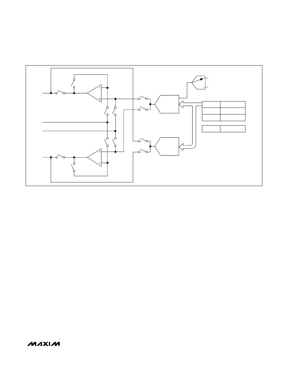
long lengths of wire. The unity-gain buffer configuration
is automatically selected, and it provides the DAC out-
put signal directly to the device pin OUTnLG. With the
large op amp selected, the small op amp can be used
as an independent device for external circuit applica-
tions when the PWM is disabled. Alternatively, the PWM
can also be enabled to drive the OUTnSM device pin,
in which case the small op amp is OFF.
Selecting the small op amp as the DAC output driver
device is useful for routing the output signal to other cir-
cuits in an embedded control system with high-imped-
ance load connections. The unity-gain buffer configuration
is automatically selected, and it provides the DAC output
signal directly to the device pin OUTnSM. With the small
op amp selected, the large op amp can be used as an
independent device for external circuit applications when
the PWM is disabled. Alternatively, the PWM can also be
enabled to drive the OUTnLG device pin, in which case
the large op amp is OFF.
The DAC has two reference voltage sources available by
selection, V
DD
and V
REF
input. When the external refer-
ence is selected (V
REF
), the actual DAC reference is 2 x
V
REF
. See V
REF
to 2.5V for nominal operation. The output
of the DAC is a voltage proportional to the reference volt-
age selected, where the proportionality scaling (DAC
input) is set in the data input register DOPn_Data.
The DOP module also provides a 12-bit digital PWM
output. At a nominal 4MHz frequency, the frequency of
the PWM is 122Hz (PWM period = 8.192ms). The DAC
and the PWM share the same input register,
DOPn_Data, where the PWM uses the 12 MSBs, in
two’s-complement format. An input of 000Xh (4 LSBs
are ignored) outputs a 50% duty cycle waveform at the
selected output pin (either OUTnSM or OUTnLG). The
PWM bit weight is 2µs, at a nominal frequency of 4MHz.
The minimum duty cycle is obtained when the input is
800Xh (duty cycle is 0 / 4096 = 0), and the maximum
duty cycle at 7FFXh (duty cycle is 4095 / 4096 =
99.98%). A new PWM input word is only effective at the
end of a current PWM cycle, therefore preventing PWM
glitches on the output.
Either the small or the large op amp in the DOP module
can also be selected as an uncommitted op amp in the
MAX1464. The op amps can be configured as a unity-
gain buffer, where the output is internally connected to the
negative terminal of the op amp, or a stand-alone op amp,
where both AMPnM and AMPnP can be externally con-
nected for various analog functions. In the case of a buffer,
the device pin AMPnM is in high-impedance mode, as the
feedback loop around the op amp is connected internally.
DAC
10h OR 13h
DOPn_Data
12h OR 15h
DOPn_Config
30h
OpAmp_Config
11h OR 14h
DOPn_Control
REF
PWM
SW0
SW1
SW2
SW3
SW4
SW5
SW6
SW7
SW8
SW9
2 x V
REF
V
DD
OUTnSM
AMPnM
AMPnP
OUTnLG
SW10
SW11
SM
LG
Figure 5. DOP1 and DOP2 Modules