Table 7. single-ended (se[3:0]), Table 8. adc_config_1a (address = 02h), Table 9. adc_config_1b (address = 03h) – Rainbow Electronics MAX1464 User Manual
Page 31
MAX1464
Low-Power, Low-Noise Multichannel
Sensor Signal Processor
______________________________________________________________________________________
31
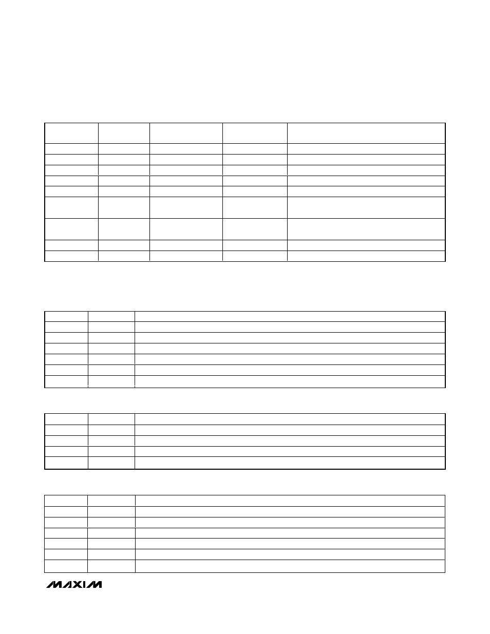
SE[3:0]
PGA
RANGE (V/V)
ADC
+INPUT
ADC
-INPUT
DESCRIPTION
0001
0.99
VBG
V
SS
Bandgap voltage.
0010
0.99 to 244
OUTnSM
V
SS
Output of small op-amp n.
0011
0.99 to 244
OUTnLG
V
SS
Output of large op-amp n.
0100
0.7*
V
DD
**
V
SS
Power-supply voltage.
0101
0.7*
V
SS
V
SS
Power-supply ground.
0110
0.7*
DACn_OUT using
OUTnSM
V
SS
DACn output through small op-amp n configured
as unity-gain buffer.
0111
0.7*
DACn_OUT using
OUTnLG
V
SS
DACn output through large op-amp n configured
as unity-gain buffer.
1000
0.99 to 244
INPn
V
SS
Single-ended input on INPn.
1001
0.99 to 244
INMn
V
SS
Single-ended input on INMn.
Table 7. Single-Ended (SE[3:0])
*The PGA operates at a fixed reduced gain of 0.7V/V to enable conversion of input signals at and near V
DD
and V
SS
. This gain set-
ting is not selectable.
**When measuring V
DD
, use the external reference or the 4 x V
BG
setting.
BIT
NAME
DESCRIPTION
15–11
PGA1[4:0]
Programmable-gain amplifier setting to use during conversion of channel 1. PGA1[4] = MSB.
10–8
CLK1[2:0]
ADC clock setting to use during conversion of channel 1. CLK1[2] = MSB.
7
—
Unused.
6–4
RES1[2:0]
ADC resolution setting to use during conversion of channel 1. RES1[2] = MSB.
3
CO1[3]
Coarse-offset sign bit.
2–0
CO1[2:0]
Coarse-offset DAC setting to use during conversion of channel 1. CO1[2] = MSB.
Table 8. ADC_Config_1A (Address = 02h)
BIT
NAME
DESCRIPTION
15–7
—
Unused.
6–4
BIAS1[2:0]
ADC bias setting to use during conversion of channel 1. BIAS1[2] = MSB.
3–2
—
Unused.
1–0
REF1[1:0]
Reference select for conversion on channel 1. REF1[1] = MSB.
Table 9. ADC_Config_1B (Address = 03h)
BIT
NAME
DESCRIPTION
15–11
PGA2[4:0]
Programmable-gain amplifier to use during conversion of channel 2. PGA[4] = MSB.
10–8
CLK2[2:0]
ADC clock setting to use during conversion of channel 2. CLK2[2] = MSB.
7
—
Unused.
6
RES2[2:0]
ADC resolution setting to use during conversion of channel 2. RES2[2] = MSB.
3
CO2[3]
Coarse-offset DAC sign bit.
2–0
CO2[2:0]
Coarse-offset DAC setting to use during conversion of channel 2. CO2[2] = MSB.
Table 10. ADC_Config_2A (Address = 05h)