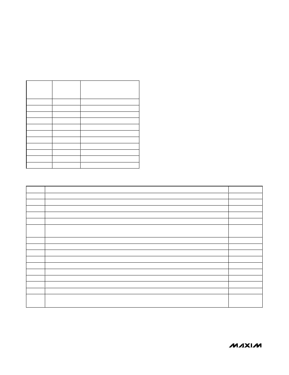
Table 39. command register (cr) decoding – Rainbow Electronics MAX1464 User Manual
Page 42
MAX1464
Low-Power, Low-Noise Multichannel
Sensor Signal Processor
42
______________________________________________________________________________________
CR
DESCRIPTION
CPU HALTED
0000
Write 16-bit DHR contents into the CPU port specified by PFAR[3:0].
No (Note 17)
0001
Write 8-bit DHR[7:0] contents into FLASH memory location specified by PFAR[11:0].
Yes
0010
Read 16-bit CPU port specified by PFAR[3:0] into DHR.
No (Note 17)
0011
Read 8-bit FLASH location specified by PFAR[11:0] into DHR[7:0].
Yes
0100
Read 16-bit CPU accumulator register (A) into DHR.
Yes
0101
Read 8-bit FLASH location specified by the CPU program counter (PC) (CPU instruction or data) to
DHR[7:0].
Yes
0110
Read 16-bit CPU PC to DHR.
Yes
0111
Halt the CPU.
No
1000
Start the CPU, i.e., clear the HALT CPU bit from the current PC location.
Yes
1001
Single step the CPU. Only one CPU clock cycle is executed.
Yes
1010
Reset the PC to zero.
Yes
1011
Reset the modules, FLASH controller, and CPU registers D, E, F.
Yes
1100
No operation.
—
1101
Erase a 64-byte “page” of FLASH as specified by PFAR[11:6].
Yes
1110
Erase the entire FLASH partition (4kB, PS0, or 128 bytes, PS1).
Yes
1111
Change from FLASH partition PS0 to FLASH partition PS1 (128 byte auxiliary). A subsequent halt
CPU command resets the partition selection back to PS0.
Yes
Table 39. Command Register (CR) Decoding
Note 17: Reading and writing the CPU ports by the serial interface is allowed while the CPU is executing its program. In the case of
simultaneous access of the ports by both the CPU and the serial interface, the CPU has priority. Although this procedure is
allowed, it is not recommended, as the serial interface may change values previously written by the CPU. If a “snapshot”
of the ports and module register contents is required while the CPU is running, halt the CPU, read the contents of the ports
and/or module registers, and restore the original port/module register values prior to starting the CPU again.
IRSA[3:0]
REGISTER
NIBBLE
ADDRESSED
DESCRIPTION
0000
DHR[3:0]
Write IRSD[3:0] to DHR[3:0].
0001
DHR[7:4]
Write IRSD[3:0] to DHR[7:4].
0010
DHR[11:8]
Write IRSD[3:0] to DHR[11:8].
0011
DHR[15:12]
Write IRSD[3:0] to DHR[15:12].
0100
PFAR[3:0]
Write IRSD[3:0] to PFAR[3:0].
0101
PFAR[7:4]
Write IRSD[3:0] to PFAR[7:4].
0110
PFAR[11:8]
Write IRSD[3:0] to PFAR[11:8].
0111
PFAR[15:12]
Write IRSD[3:0] to PFAR[15:12].
1000
CR[3:0]
Write IRSD[3:0] to CR[3:0].
1001
IMR[3:0]
Write IRSD[3:0] to IR[3:0].
1010–1110
—
Unused.
Table 38. Internal Register Set Address
(IRSA) Decoding