On-chip temperature sensing, Output format, Initialization – Rainbow Electronics MAX1464 User Manual
Page 13: Power-on reset (por), Cpu architecture, Cpu registers
MAX1464
Low-Power, Low-Noise Multichannel
Sensor Signal Processor
______________________________________________________________________________________
13
On-Chip Temperature Sensing
The on-chip temperature sensor changes +2mV/°C over
the operating range. The ADC converts the temperature
sensor in a similar manner as the sensor inputs. During
an ADC conversion of the temperature sensor, the ADC
automatically uses four times the internal 1.25V reference
as the ADC full-scale reference (5V). The temperature
data format is 15-bit plus sign in two’s-complement for-
mat. Gain offset compensation can be programmed to
utilize the full-scale range of the ADC. Offset compensa-
tion by the CO DAC is provided so that the nominal tem-
perature measurement can be centered at the ADC
output value. Use the CPU to provide additional digital
gain and offset correction.
Output Format
There are two output modules in the MAX1464—DOP1
(DAC Op Amp PWM 1) and DOP2 (DAC Op Amp PWM
2). Each of the DOP modules contains a 16-bit DAC, a
12-bit digital PWM converter, a small op amp, and a
large op amp with high-output-drive capability. Each
module can be configured in several different modes to
suit a wide range of output signal requirements. Either
the DAC or the PWM can be selected as the primary
output signal. The DAC output signal must be routed to
one of the two op amps before being made available to
a device pin. See the DAC, Op Amp, PWM Modules
(DPOn) section for details. Additional digital outputs are
available on the GPIOs.
Initialization
A user-defined initialization routine is required to config-
ure the oscillator frequency and various analog modules,
e.g., PGA gain, ADC resolution, ADC clock settings, etc.
After the initialization routine, the CPU can start execution
of the main program.
Power-On Reset (POR)
The MAX1464 contains a POR circuit to disable CPU
execution until adequate V
DD
and V
DDF
voltage are
available for operation. Once the power-on state has
been reached, the MAX1464 is kept under reset condi-
tion for 250µs before the CPU starts execution. Below
the POR threshold, all internal CPU registers are set to
their POR default state. Power-on control bits for internal
modules are reset to the OFF condition.
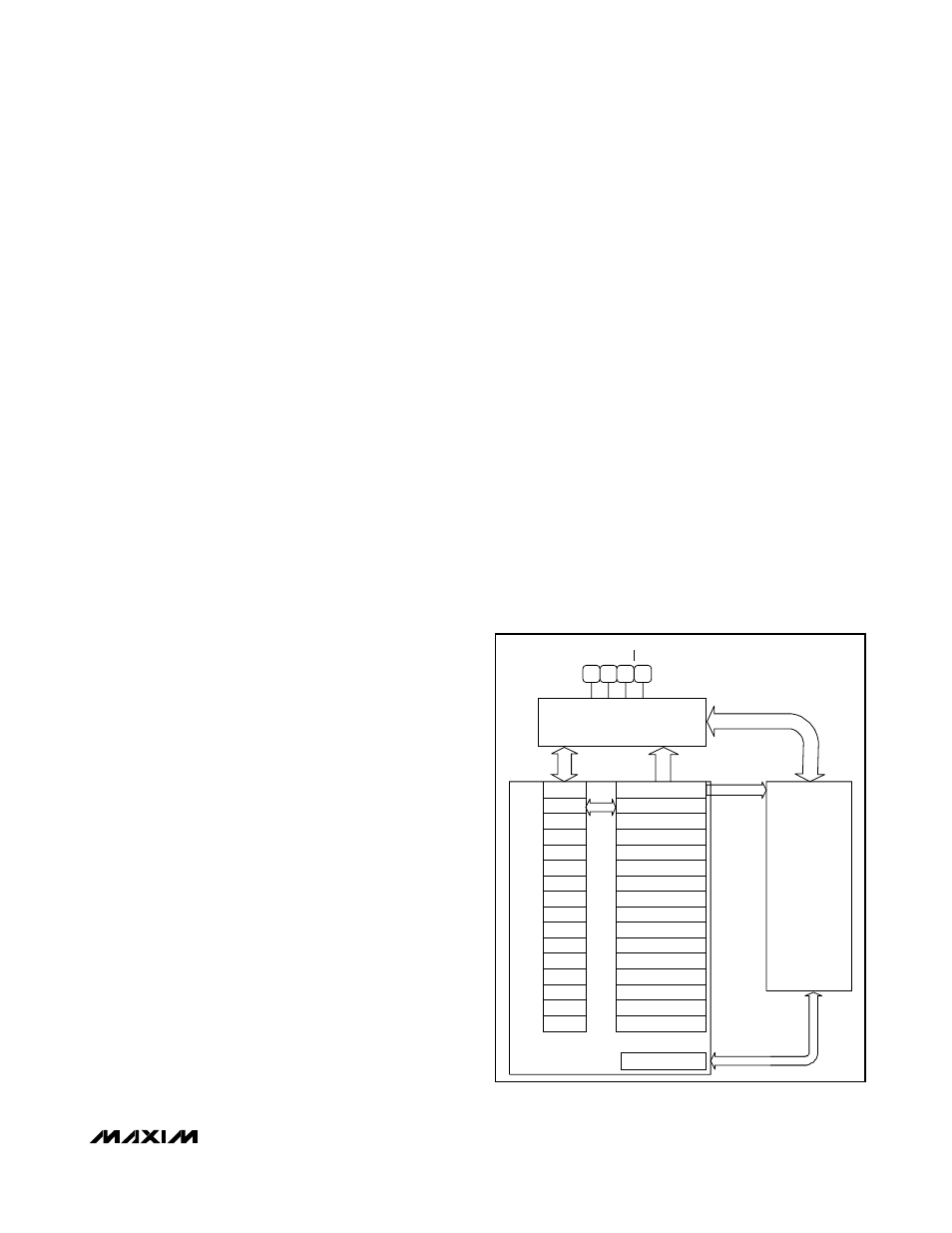
CPU Architecture
The CPU provides a wide range of functionality to be
incorporated in an embedded system. The CPU can
compensate nonlinear and temperature-dependent sen-
sors, check for over/underlimit conditions, output sensor
or temperature data as an analog signal or pulse-width-
modulated digital signal, and execute control strategies.
The CPU can perform a limited amount of signal pro-
cessing (filtering). A timer is included so that uniform
sampling (equally spaced ADC conversions) of the
input sensors can be performed.
The CPU registers and ports are implemented in volatile,
static memory. There are several registers contained in
various peripheral modules that provide module configu-
ration settings, control functions, and data. These module
registers are accessible through an indirect addressing
scheme as described in detail in the CPU Registers,
CPU Ports, and Modules sections. Figure 3 shows the
CPU architecture.
CPU Registers
The MAX1464 incorporates a CPU with 16 internal regis-
ters. All the CPU registers have a 16-bit data word width.
Five of the 16 registers have predefined functional oper-
ations that are dependent on the instruction being exe-
cuted. The remaining registers are general purpose.
The CPU registers are embedded in the CPU itself and
are not all directly accessible by the serial interface. The
accumulator register (A), the pointer register (P), and the
instruction (FLASH data) can be read through the serial
interface when the CPU is halted. This enables a single-
FLASH MEMORY
(4kB)
SERIAL INTERFACE
SCLK
DI
DO
CS
R0 POINTER (P)
R1 ACCUMULATOR (A)
R2
R3 MULTIPLICAND (N)
R4 MULTIPLIER (M)
R6
R7
R8
R9
RA
RB
RC
RD
RE
RF
P0
P1
P2
P1
P3
P4
P5
P6
P7
P8
PA
PB
PC
PD
PE
PF
CPU REGISTERS
INSTRUCTION
CPU
FLASH DATA
ADDRESS
CPU PORTS
R5 INDEX (I)
Figure 3. CPU Architecture