Max3645, Detailed description, Pin description – Rainbow Electronics MAX3645 User Manual
Page 6
MAX3645
Detailed Description
The MAX3645 consists of gain stages, offset correction,
power detector, LOS indicators, and PECL output buffers.
See Figure 2 for the functional diagram.
Data Input
The data inputs have a single-ended input resistance of
4.8k
Ω and are internally DC-biased to V
CC
- 0.87V (see
Figure 3). External capacitors are required to AC-cou-
ple the data signals. Pattern-dependent jitter is mini-
mized by using coupling capacitor values large enough
to pass the lowest frequencies of interest (consecutive
ones and zeros) with the given input resistance.
Typically, 0.1µF coupling capacitors yield a -3dB fre-
quency of 354Hz. Capacitor tolerance and input resis-
tance variation (3.3k
Ω to 6.4kΩ) must be considered to
accurately calculate the -3dB frequency. Capacitor val-
ues should be chosen that set the -3dB frequency at
least a factor of 10 below the lowest frequency of inter-
est. A capacitor value of 0.1µF is recommended.
Gain Stage and Offset Correction
The limiting amplifier provides approximately 74dB
(R
TH
= 100
Ω) of gain. This large gain makes the ampli-
fier susceptible to small DC offsets in the signal path.
To correct DC offsets, the amplifier has an internal feed-
back loop that acts as a DC autozero circuit. By cor-
recting the DC offsets, the limiting amplifier improves
receiver sensitivity and power-detector accuracy.
+2.97V to +5.5V, 125Mbps to 200Mbps Limiting
Amplifier with Loss-of-Signal Detector
6
_______________________________________________________________________________________
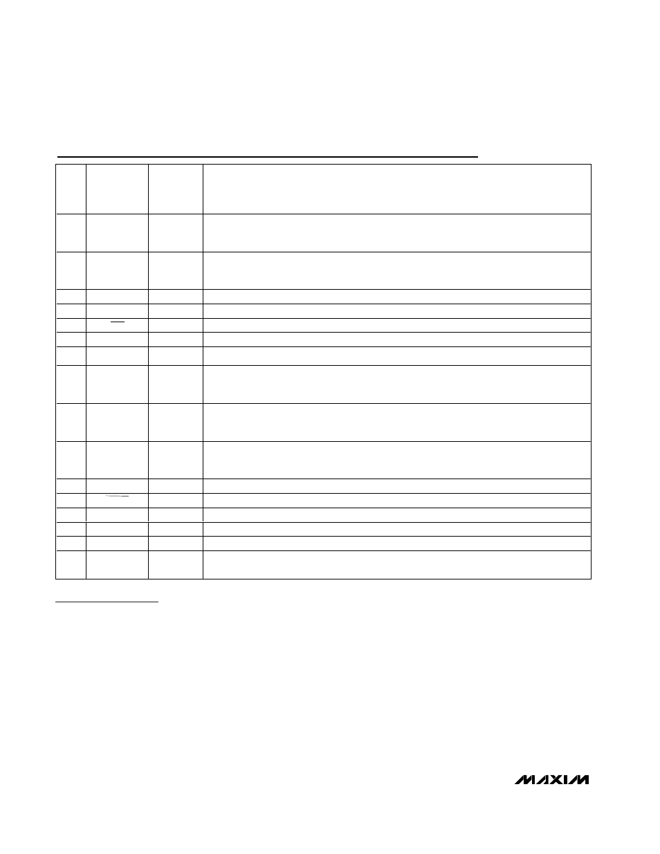
PIN
MINDSPEED
MC2045-2
MC2045-2Y
PIN NAME
MAXIM
MAX3645
PIN NAME
FUNCTION
1
CAZ-
CAZ2
Offset-Correction-Loop Capacitor Connection. A capacitor connected between this pin and
CAZ1 sets the time constant of the offset correction loop. The offset correction is disabled
when the CAZ1 and CAZ2 pins are shorted together.
2
CAZ+
CAZ1
Offset-Correction-Loop Capacitor Connection. A capacitor connected between this pin and
CAZ2 sets the time constant of the offset correction loop. The offset correction is disabled
when the CAZ2 and CAZ1 pins are shorted together.
3
GNDA
GNDA
Analog Supply Ground. Must be at the same potential as the GNDE pin.
4
D
IN
DIN+
Positive Data Input
5
D
IN
DIN-
Negative Data Input
6
V
CCA
V
CCA
+2.97V to +5.5V Analog Supply Voltage. Must be at same potential as the V
CCE
pin.
7
C
F
CSD
S i g nal - D etect- Fi l ter C ap aci tor C onnecti on. C onnect the C
S D
cap aci tor b etw een C S D and V
C C A
.
8
JAM
DIS
Disable Input, PECL or CMOS Compatible. Data outputs are held to a static logic 0 when DIS is
asserted high. The LOS function remains active when the outputs are disabled. When
connected to the LOS pin, an automatic squelch function is enabled.
9
ST
LOS
Positive Loss-of-Signal Output, PECL. LOS is high when the level of the input signal drops
below the threshold set by the TH input. LOS is low when the signal level is above the
threshold. LOS can be connected directly to DIS for automatic squelch.
10
ST
LOS
Negative Loss-of-Signal Output, PECL. LOS is low when the level of the input signal drops
below the threshold set by the TH input. LOS is high when the signal level is above the
threshold.
11
GNDE
GNDE
Digital Supply Ground. Must be at the same potential as the GNDA pin.
12
D
OUT
DOUT-
Negative Data Output, PECL. A high at DIS forces DOUT- high.
13
D
OUT
DOUT+
Positive Data Output, PECL. A high at DIS forces DOUT+ low.
14
V
CCE
V
CCE
+2.97V to +5.5V Digital Supply Voltage. Must be at the same potential as the V
CCA
pin.
15
NC
N.C.
No Connection
16
V
SET
TH
Loss-of-Signal Threshold Pin. Resistor (R
TH
) to ground sets the LOS threshold. This pin cannot
be left open.
Pin Description