Rainbow Electronics MAX3645 User Manual
Page 2
MAX3645
+2.97V to +5.5V, 125Mbps to 200Mbps Limiting
Amplifier with Loss-of-Signal Detector
2
_______________________________________________________________________________________
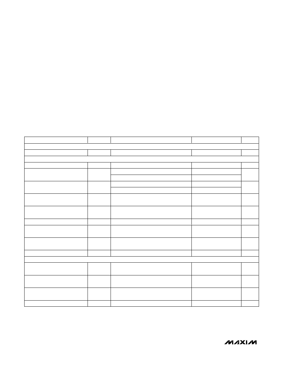
ABSOLUTE MAXIMUM RATINGS
ELECTRICAL CHARACTERISTICS
(V
CC
= +2.97V to +5.5V, PECL outputs are terminated with 50
Ω to V
CC
- 2V, R
TH
= 100
Ω, C
AZ
= 0.1µF, C
SD
= 1nF, T
A
= -40°C to
+85°C. Typical values are at V
CC
= +3.3V, T
A
= +25°C, unless otherwise noted.)
Stresses beyond those listed under “Absolute Maximum Ratings” may cause permanent damage to the device. These are stress ratings only, and functional
operation of the device at these or any other conditions beyond those indicated in the operational sections of the specifications is not implied. Exposure to
absolute maximum rating conditions for extended periods may affect device reliability.
Power-Supply Voltage (V
CCA
, V
CCE
) ....................-0.5V to +7.0V
Voltage at CAZ1, CAZ2, DIN+,
DIN-, CSD, DIS, TH ................................-0.5V to (V
CC
+ 0.5V)
PECL Output Current (DOUT+, DOUT-, LOS, LOS) ...........50mA
Differential Voltage between CAZ1 and CAZ2......-1.5V to +1.5V
Differential Voltage between DIN+ and DIN- ........-1.5V to +1.5V
Continuous Power Dissipation (T
A
= +85
°C)
16-Pin SO (derate 8.7mW/
°C above +85°C)................565mW
16-Pin QSOP (derate 8.3mW/
°C above +85°C)...........540mW
Storage Ambient Temperature Range (T
S
)…….-65
°C to +160°C
Lead Temperature (soldering, 10s)...........……………….+300
°C
PARAMETER
SYM B O L CONDITIONS
MIN
TYP
MAX
UNITS
POWER SUPPLY
Supply Current
I
CC
Excludes PECL termination currents
18
27
mA
INPUT SPECIFICATIONS
Input Resistance
R
IN
Single ended; V
IN
= ±200mV
3.3
4.8
6.4
k
Ω
Single ended
0.5
Input Sensitivity (Note 1)
V
IN-MIN
Differential
1.0
mV
P-P
Single ended
750
Input Overload (Note 1)
V
IN-MAX
Differential
1500
mV
P-P
Input-Referred Offset Voltage
Unterminated input, output offset divided by
DC gain (Note 2)
2
40
µV
Input Common-Mode Voltage
V
CMM
V
CC
-
0.87
V
Input-Referred RMS Noise
V
IN-NOISE
(Notes 2, 3)
36
50
µV
RMS
DIS Input High
V
IH
PECL or CMOS logic
V
CC
-
1160
V
CC
mV
DIS Input Low
V
IL
PECL or CMOS logic
0
V
CC
-
1480
mV
DIS Input Current
I
IL
, I
IH
0V
≤ V
DIS
≤ V
CC
-10
+10
µA
OUTPUT SPECIFICATIONS
PECL Output-Voltage High
(Notes 1, 2)
V
CC
-
1085
V
CC
-
880
mV
PECL Output-Voltage Low
(Notes 1, 2)
V
CC
-
1830
V
CC
-
1555
mV
Data Output Transition Time
t
R
, t
F
20% to 80% (Notes 1, 2, 4)
0.7
1.4
ns
Pulse-Width Distortion
PWD
(Notes 1, 2, 4, 5)
30
200
ps