Rainbow Electronics MAX3645 User Manual
General description, Applications, Features
General Description
The MAX3645 limiting amplifier functions as a data
quantizer and is pin compatible with the Mindspeed
MC2045-2 and MC2045-2Y postamplifiers. The amplifi-
er accepts a wide range of input voltages and provides
constant-level positive emitter-coupled logic (PECL)
output voltages with controlled edge speeds.
The MAX3645 features an integrated power detector
with complementary PECL loss-of-signal (LOS) outputs
that indicate when the input power level drops below a
programmable threshold. An optional squelch function
holds the data outputs at static levels during a
LOS condition.
The MAX3645 operates from a single +3.3V or +5.0V
power supply over a -40
°C to +85°C temperature
range. It is available in 16-pin SO and 16-pin QSOP
packages.
Applications
SONET 155Mbps Transceivers
Fast Ethernet Receivers
FDDI 125Mbps Receivers
FTTx Receivers
ESCON Receivers
Features
♦ Pin Compatible with the Mindspeed
MC2045-2/MC2045-2Y
♦ 500µV Input Sensitivity (BER = 10
-12
)
♦ Compatible with 4B/5B Data Coding
♦ Programmable LOS Threshold
♦ Stable LOS Threshold Over Supply Range
♦ Output Disable Function and Automatic Squelch
♦ Single +3.3V or +5.0V Power Supply
♦ 18mA Supply Current
MAX3645
+2.97V to +5.5V, 125Mbps to 200Mbps Limiting
Amplifier with Loss-of-Signal Detector
________________________________________________________________ Maxim Integrated Products
1
Ordering Information
19-3026; Rev 0; 10/03
For pricing, delivery, and ordering information, please contact Maxim/Dallas Direct! at
1-888-629-4642, or visit Maxim’s website at www.maxim-ic.com.
PART
TEMP RANGE
PIN-PACKAGE
MAX3645ESE
-40°C to +85°C
16 SO
MAX3645EEE
-40
°C to +85°C
16 QSOP
16
15
14
13
12
11
10
9
1
2
3
4
5
6
7
8
CAZ2
TH
N.C.
V
CCE
DOUT+
DOUT-
GNDE
LOS
TOP VIEW
MAX3645
SO/QSOP
CAZ1
GNDA
V
CCA
DIN+
DIN-
CSD
DIS
LOS
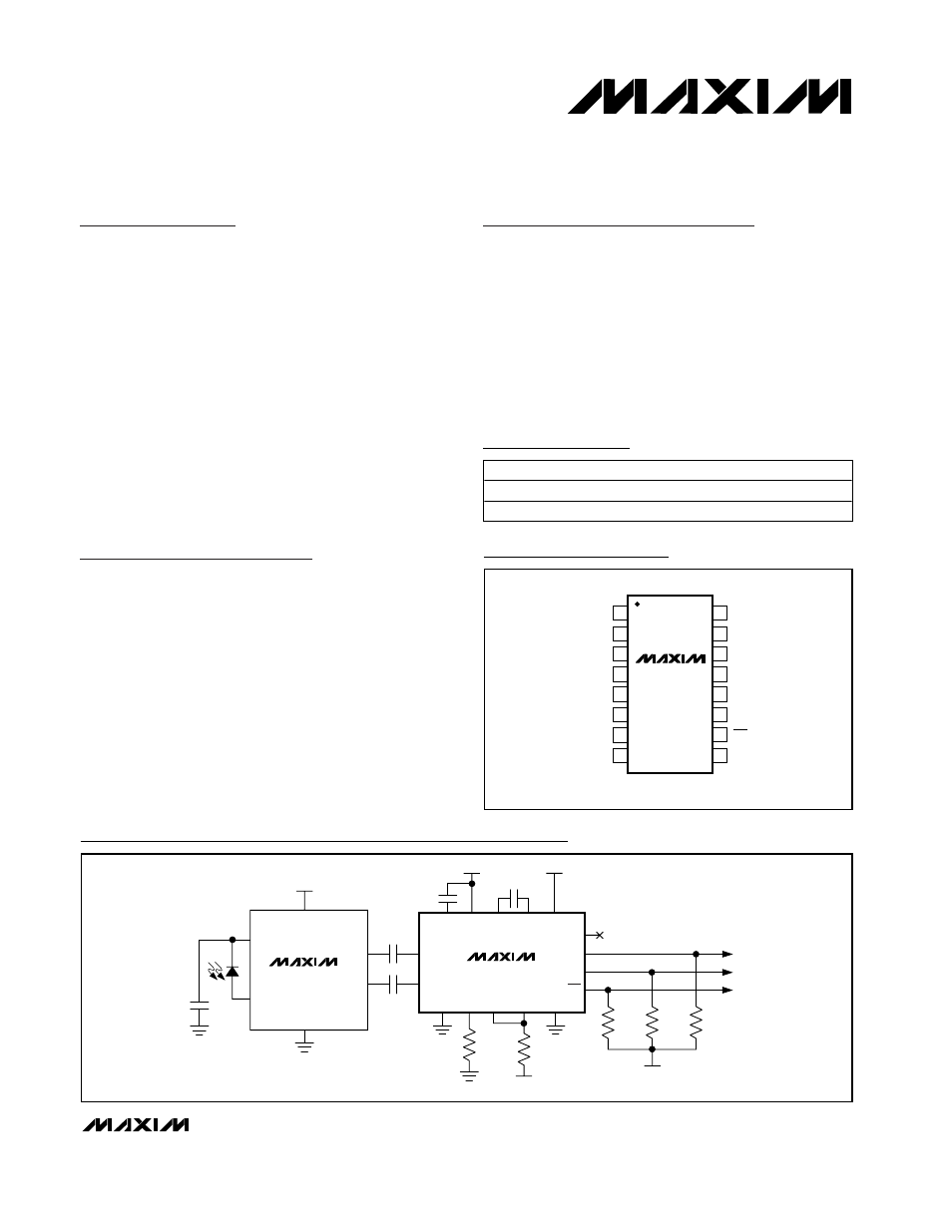
Pin Configuration
MAX3645
MAX3644*
PIN K
IN
V
CC
V
CC
V
CC
V
CC
OUT-
OUT+
DIN+
DIN-
GNDA
DOUT+
DOUT-
LOS
LOS
DIS
CSD V
CCA
CAZ1
CAZ2
GND
*FUTURE PRODUCT
V
CCE
TH
GNDE
N.C.
0.1
µF
0.1
µF
C
SD
1nF
C
AZ
0.1
µF
R
TH
100
Ω
50
Ω
50
Ω
50
Ω
50
Ω
V
CC
- 2V
V
CC
- 2V
Typical Application Circuit