Rapids implementation – Rainbow Electronics AT25DF081A User Manual
Page 42
42
8715C–SFLSH–11/2012
AT25DF081A
13.
RapidS Implementation
To implement RapidS and operate at clock frequencies higher than what can be achieved in a viable SPI imple-
mentation, a full clock cycle can be used to transmit data back and forth across the serial bus. The AT25DF081A is
designed to always clock its data out on the falling edge of the SCK signal and clock data in on the rising edge of
SCK.
For full clock cycle operation to be achieved, when the AT25DF081A is clocking data out on the falling edge of
SCK, the host controller should wait until the next falling edge of SCK to latch the data in. Similarly, the host con-
troller should clock its data out on the rising edge of SCK in order to give the AT25DF081A a full clock cycle to latch
the incoming data in on the next rising edge of SCK.
Implementing RapidS allows a system to run at higher clock frequencies since a full clock cycle is used to accom-
modate a device’s clock-to-output time, input setup time, and associated rise/fall times. For example, if the system
clock frequency is 100 MHz (10ns cycle time) with a 50% duty cycle, and the host controller has an input setup
time of 2ns, then a standard SPI implementation would require that the slave device be capable of outputting its
data in less than 3ns to meet the 2ns host controller setup time [(10ns x 50%) – 2ns] not accounting for rise/fall
times. In an SPI mode 0 or 3 implementation, the SPI master is designed to clock in data on the next immediate ris-
ing edge of SCK after the SPI slave has clocked its data out on the preceding falling edge. This essentially makes
SPI a half-clock cycle protocol and requires extremely fast clock-to-output times and input setup times in order to
run at high clock frequencies. With a RapidS implementation of this example, however, the full 10ns cycle time is
available which gives the slave device up to 8ns, not accounting for rise/fall times, to clock its data out. Likewise,
with RapidS, the host controller has more time available to output its data to the slave since the slave device would
be clocking that data in a full clock cycle later.
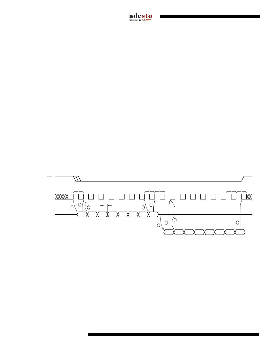
Figure 13-1. RapidS Operation
SCK
MOSI
MISO
t
V
1
2
3
4
5
6
7
8
1
2
3
4
5
6
7
8
MOSI = Master Out, Slave In
MISO = Master In, Slave Out
The Master is the ASIC/MCU and the Slave is the memory device
The Master always clocks data out on the rising edge of SCK and always clocks data in on the falling edge of SCK
The Slave always clocks data out on the falling edge of SCK and always clocks data in on the rising edge of SCK
A. Master clocks out first bit of BYTE A on the rising edge of SCK
B. Slave clocks in first bit of BYTE A on the next rising edge of SCK
C. Master clocks out second bit of BYTE A on the same rising edge of SCK
D. Last bit of BYTE A is clocked out from the Master
E. Last bit of BYTE A is clocked into the slave
F. Slave clocks out first bit of BYTE B
G. Master clocks in first bit of BYTE B
H. Slave clocks out second bit of BYTE B
I.
Master clocks in last bit of BYTE B
A
B
C
D
E
F
G
1
H
BYTE A
MSB
LSB
BYTE B
MSB
LSB
Slave
CS
I