Rainbow Electronics AT25DF081A User Manual
Page 29
29
8715C–SFLSH–11/2012
AT25DF081A
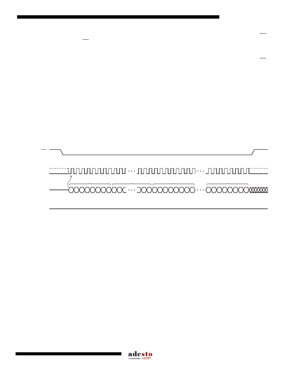
The three address bytes and at least one complete byte of data must be clocked into the device before the CS pin
is deasserted, and the CS pin must be deasserted on even byte boundaries (multiples of eight bits); otherwise, the
device will abort the operation and the user-programmable portion of the OTP Security Register will not be pro-
grammed. The WEL bit in the Status Register will be reset back to the logical “0” state if the OTP Security Register
program cycle aborts due to an incomplete address being sent, an incomplete byte of data being sent, the CS pin
being deasserted on uneven byte boundaries, or because the user-programmable portion of the OTP Security
Register was previously programmed.
While the device is programming the OTP Security Register, the Status Register can be read and will indicate that
the device is busy. For faster throughput, it is recommended that the Status Register be polled rather than waiting
the t
OTPP
time to determine if the data bytes have finished programming. At some point before the OTP Security
Register programming completes, the WEL bit in the Status Register will be reset back to the logical “0” state.
If the device is powered-down during the OTP Security Register program cycle, then the contents of the 64-byte
user programmable portion of the OTP Security Register cannot be guaranteed and cannot be programmed again.
The Program OTP Security Register command utilizes the internal 256-buffer for processing. Therefore, the con-
tents of the buffer will be altered from its previous state when this command is issued.
Figure 10-4. Program OTP Security Register
SCK
CS
SI
SO
MSB
MSB
2
3
1
0
1
0
0
1
1
0
1
1
6
7
5
4
9
8
39
37 38
33
36
35
34
31 32
29 30
OPCODE
HIGH-IMPEDANCE
A
A
A
A
A
A
MSB
D
D
D
D
D
D
D
D
ADDRESS BITS A23-A0
DATA IN BYTE 1
MSB
D
D
D
D
D
D
D
D
DATA IN BYTE n