Digital timing characteristics – Rainbow Electronics ATA5746 User Manual
Page 38
38
4596A–RKE–05/06
ATA5745/ATA5746 [Preliminary]
16. Digital Timing Characteristics
All parameters refer to GND and are valid for T
amb
= –40°C to +105°C, V
VS3V_AVCC
= V
VS5V
= 2.7V to 3.3V, and V
VS5V
= 4.5V to 5.5V.
Typical values are given at V
VS3V_AVCC
= V
VS5V
= 3V, T
amb
= 25°C, and f
RF
= 433.92 MHz unless otherwise specified. Details about current
consumption, timing, and digital pin properties can be found in the specific sections of the “Electrical Characteristics”
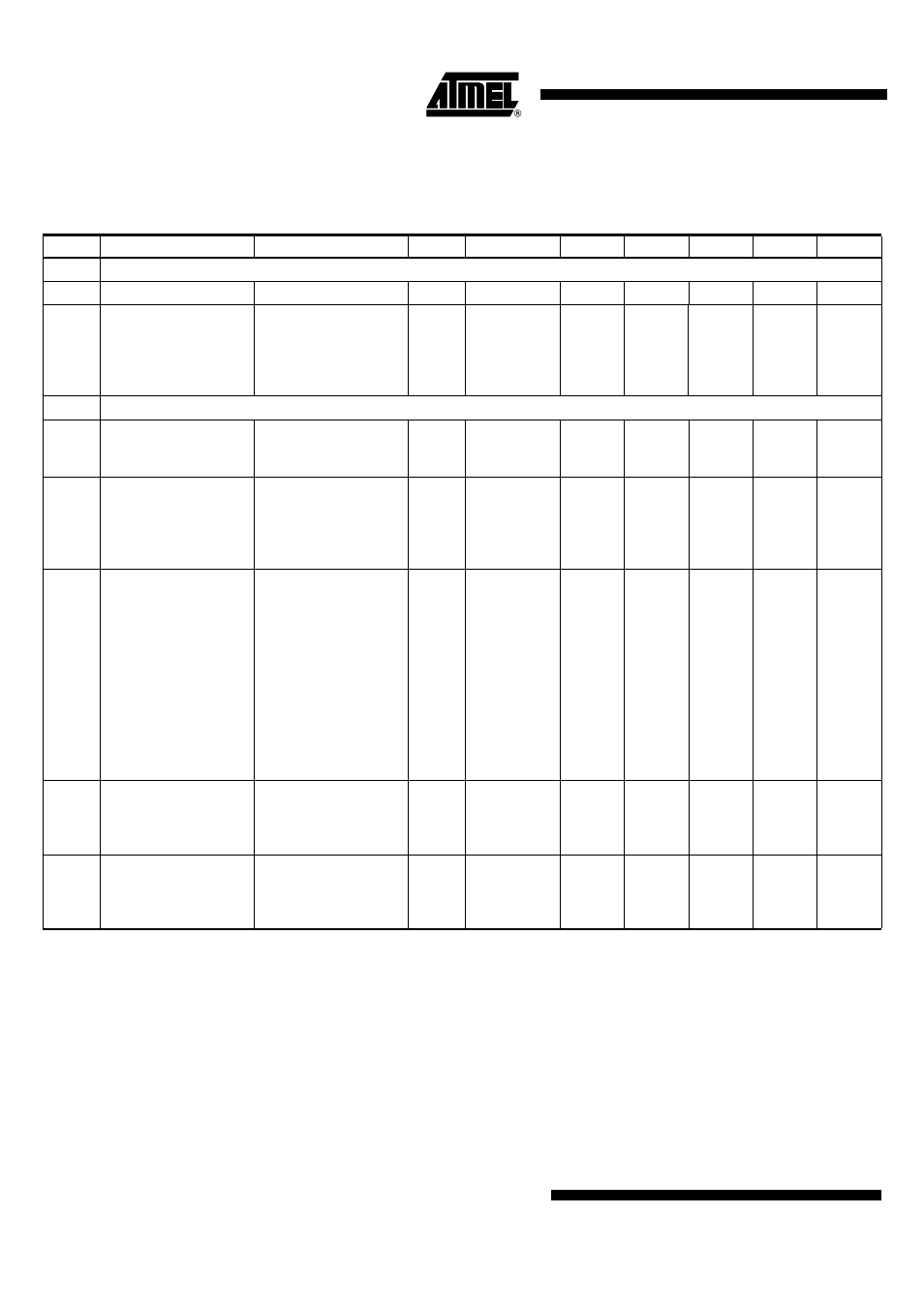
No.
Parameters
Test Conditions
Pin
Symbol
Min.
Typ.
Max.
Unit
Type*
9
Basic Clock Cycle of the Digital Circuitry
9.1
Basic clock cycle
T
DCLK
16 / f
XTO
16 / f
XTO
µs
A
9.2
Extended basic clock
cycle
BR_Range_0
BR_Range_1
BR_Range_2
BR_Range_3
T
XDCLK
8
4
2
1
× T
DCLK
8
4
2
1
× T
DCLK
µs
A
10
Active Mode
10.1
Startup PLL
T
Startup_PLL
15 µs +
208
×
T
DCLK
µs
A
10.2
Startup signal
processing
BR_Range_0
BR_Range_1
BR_Range_2
BR_Range_3
T
Startup_Sig_Proc
929.5
545.5
353.5
257.5
× T
DCLK
929.5
545.5
353.5
257.5
× T
DCLK
A
10.3
Bit rate range
ASK
BR_Range =
BR_Range0
BR_Range1
BR_Range2
BR_Range3
FSK
BR_Range =
BR_Range0
BR_Range1
BR_Range2
BR_Range3
BR_Range
1.0
2.0
4.0
8.0
1.0
2.0
4.0
8.0
2.5
5.0
10.0
10.0
2.5
5.0
10.0
20.0
Kbits/s
A
10.4
Minimum time period
between edges at pin
DATA_OUT
BR_Range_0
BR_Range_1
BR_Range_2
BR_Range_3
24
T
DATA_OUT_min
10
×
T
XDCLK
µs
A
10.5
Edge-to-edge time
period of the data signal
for full sensitivity in
Active mode
BR_Range_0
BR_Range_1
BR_Range_2
BR_Range_3
T
DATA_OUT
200
100
50
25
500
250
125
62.5
µs
B
*) Type means: A = 100% tested, B = 100% correlation tested, C = Characterized on samples, D = Design parameter