8 rssi output – Rainbow Electronics ATA5746 User Manual
Page 13

13
4596A–RKE–05/06
ATA5745/ATA5746 [Preliminary]
The ATA5745/ATA5746 can also receive FSK and ASK modulated signals if they are much
higher than the I1dBCP. It can typically receive useful signals at
–
10 dBm. This is often referred
to as the nonlinear dynamic range (that is, the maximum to minimum receiving signal), and is
95 dB for 10 Kbits/s Manchester (FSK). This value is useful if the transmitter and receiver are
very close to each other.
2.7
In-band Disturbers, Data Filter, Quasi-peak Detector, Data Slicer
If a disturbing signal falls into the received band, or if a blocker is not a continuous wave, the
performance of a receiver strongly depends on the circuits after the IF filter. Hence, the demod-
ulator, data filter, and data slicer are important.
The data filter of the ATA5745/ATA5746 functions also as a quasi-peak detector. This results in a
good suppression of above mentioned disturbers and exhibits a good carrier-to-noise perfor-
mance. The required useful-signal-to-disturbing-signal ratio, at a BER of 10
–3,
is less than 14 dB
in ASK mode and less than 3 dB (BR_Range_0 to BR_Range_2) and 6 dB (BR_Range_3) in
FSK mode. Due to the many different possible waveforms, these numbers are measured for the
signal, as well as for disturbers, with peak amplitude values. Note that these values are
worst-case values and are valid for any type of modulation and modulating frequency of the dis-
turbing signal, as well as for the receiving signal. For many combinations, lower
carrier-to-disturbing-signal ratios are needed.
2.8
RSSI Output
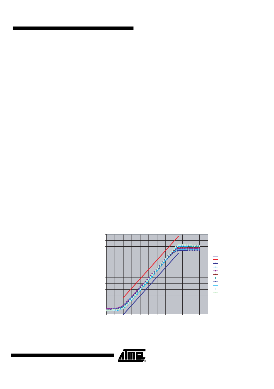
The output voltage of the pin RSSI is an analog voltage, proportional to the input power level.
Using the RSSI output signal, the signal strength of different transmitters can be distinguished.
The usable dynamic range of the RSSI amplifier is 65 dB, the input power range P(RF
IN
) is
–110 dBm to –45 dBm, and the gain is 15 mV/dB.
shows the RSSI characteristic of a
typical device at 315 MHz with VS3V_AVCC = VS5V = 2.7V to 3.3V and T
amb
= –40°C to
+105°C with a matched input as shown in
. At 433.92 MHz,
1 dB more signal level is needed for the same RSSI results.
Figure 2-9.
Typical RSSI Characteristic at 315 MHz Versus Temperature and Supply Voltage
0.4
0.5
0.6
0.7
0.8
0.9
1.0
1.1
1.2
1.3
1.4
1.5
1.6
1.7
-130
-120
-110
-100
-90
-80
-70
-60
-50
-40
-30
-20
-10
Pin (dBm)
V_
RSSI
(
V
)
max; +9dB
2.7V, -40˚C
3.0V, -40˚C
3.3V, -40˚C
2.7V, 27˚C
3.0V, 27˚C
3.3V, 27˚C
2.7V, 105˚C
3.0V, 105˚C
3.3V, 105˚C
min; -9dB
