1 pin clk_out, 2 basic clock cycle of the digital circuitry – Rainbow Electronics ATA5746 User Manual
Page 17
17
4596A–RKE–05/06
ATA5745/ATA5746 [Preliminary]
3.1
Pin CLK_OUT
Pin CLK_OUT is an output to clock a connected microcontroller. The clock is available in
Stand by a nd Active m odes. Th e frequ ency f
C L K _ O U T
can b e a djusted via the pins
CLK_OUT_CTRL0 and CLK_OUT_CTRL1, and is calculated as follows:
The signal at CLK_OUT output has a nominal 50% duty cycle. To save current, it is recom-
mended that CLK_OUT be switched off during Standby mode.
3.2
Basic Clock Cycle of the Digital Circuitry
The complete timing of the digital circuitry is derived from one clock. As seen in
, this clock cycle, T
DCLK
, is derived from the crystal oscillator (XTO) in combination with a
divider.
T
DCLK
controls the following application relevant parameters:
- Debouncing of the data signal stream
- Start-up time of the RX signal path
The start-up time and the debounce characteristic depend on the selected bit rate range
(BR_Range) which is defined by pins BR0 and BR1. The clock cycle T
XDCLK
is defined by the fol-
lowing formulas for further reference:
BR_Range
⇒
BR_Range 0: T
XDCLK
= 8
× T
DCLK
BR_Range 1: T
XDCLK
= 4
× T
DCLK
BR_Range 2: T
XDCLK
= 2
× T
DCLK
BR_Range 3: T
XDCLK
= 1
× T
DCLK
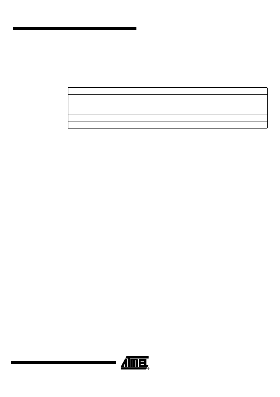
Table 3-2.
Setting of f
CLK_OUT
CLK_OUT_CTRL1
CLK_OUT_CTRL0
Function
0
0
Clock on pin CLK_OUT is switched off
(Low level on pin CLK_OUT)
0
1
f
CLK_OUT
= f
XTO
/ 3
1
0
f
CLK_OUT
= f
XTO
/ 6
1
1
f
CLK_OUT
= f
XTO
/ 12
f
DCLK
f
XTO
16
-----------
=