Electrical characteristics: general (continued) – Rainbow Electronics ATA5746 User Manual
Page 32
32
4596A–RKE–05/06
ATA5745/ATA5746 [Preliminary]
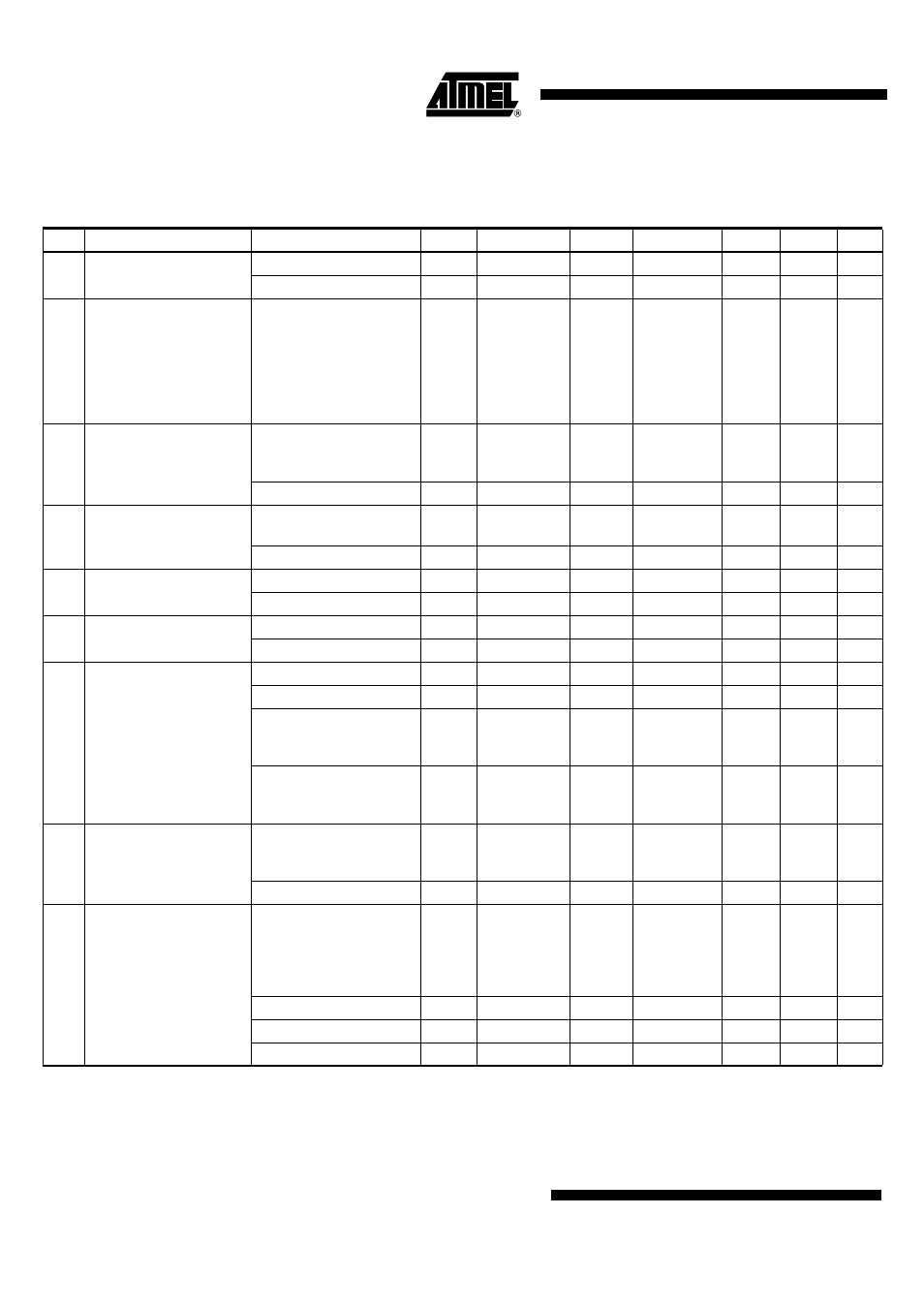
3.11 Intermediate frequency
f
RF
= 433.92 MHz
f
IF
440
kHz
A
f
RF
= 315 MHz
f
IF
440
kHz
A
3.12 System bandwidth
3 dB bandwidth
This value is for
information only!
Note that for crystal and
system frequency offset
calculations,
∆f
OFFSET
must be used.
(14)
SBW
435
kHz
A
3.13
System out-band
3rd-order input intercept
point
∆f
meas1
= 1.8 MHz
∆f
meas2
= 3.6 MHz
f
RF
= 315 MHz
(14)
IIP3
–24
dBm
C
f
RF
= 433.92 MHz
(14)
IIP3
–23
dBm
C
3.14
System outband input
1-dB compression point
∆f
meas1
= 1 MHz
f
RF
= 315 MHz
(14)
I1dBCP
–31
–36
dBm
C
f
RF
= 433.92 MHz
(14)
I1dBCP
–30
–35
dBm
C
3.15 LNA input impedance
f
RF
= 315 MHz
14
Z
in_LNA
(72.4 – j298)
Ω
C
f
RF
= 433.92 MHz
14
Z
in_LNA
(55 – j216)
Ω
C
3.16
Maximum peak RF input
level, ASK and FSK
BER < 10
–
3
, ASK: 100%
(14)
P
IN_max
+5
–10
dBm
C
FSK: f
DEV
= ±38 kHz
(14)
P
IN_max
+5
–10
dBm
C
3.17 LO spurs at LNA_IN
f < 1 GHz
(14)
–57
dBm
C
f >1 GHz
(14)
–47
dBm
C
f
LO
= 315.44 MHz
2
× f
LO
4
× f
LO
(14)
–90
–94
–68
dBm
C
f
LO
= 434.36 MHz
2
× f
LO
4
× f
LO
(14)
–92
–88
–58
dBm
C
3.18 Image rejection
With the complete image
band
f
RF
= 315 MHz
(14)
24
30
dB
A
f
RF
= 433.92 MHz
(14)
24
30
dB
A
3.19
Useful signal to interferer
ratio
Peak level of useful signal
to peak level of interferer
for BER < 10
–
3
with any
modulation scheme of
interferer
FSK BR_Ranges 0, 1, 2
(14)
SNR
FSK0-2
2
3
dB
B
FSK BR_Range_3
(14)
SNR
FSK3
4
6
dB
B
ASK (P
RF
< P
RFIN_High
)
(14)
SNR
ASK
10
14
dB
B
13. Electrical Characteristics: General (Continued)
All parameters refer to GND and are valid for T
amb
= –40°C to +105°C, V
VS3V_AVCC
= V
VS5V
= 2.7V to 3.3V, and V
VS5V
= 4.5V to 5.5V.
Typical values are given at V
VS3V_AVCC
= V
VS5V
= 3V, T
amb
= 25°C, and f
RF
= 315 MHz unless otherwise specified. Details about current
consumption, timing, and digital pin properties can be found in the specific sections of the “Electrical Characteristics”.
No. Parameters
Test Conditions
Pin
(1)
Symbol
Min.
Typ.
Max.
Unit
Type*
*) Type means: A = 100% tested, B = 100% correlation tested, C = Characterized on samples, D = Design parameter
Note:
1. Pin numbers in parenthesis were measured with RF_IN matched to 50
Ω according to
Figure 2-1 on page 6
with component
values as in
Table 2-2 on page 6
(RF
IN
).