Rainbow Electronics ATA5746 User Manual
Page 15
15
4596A–RKE–05/06
ATA5745/ATA5746 [Preliminary]
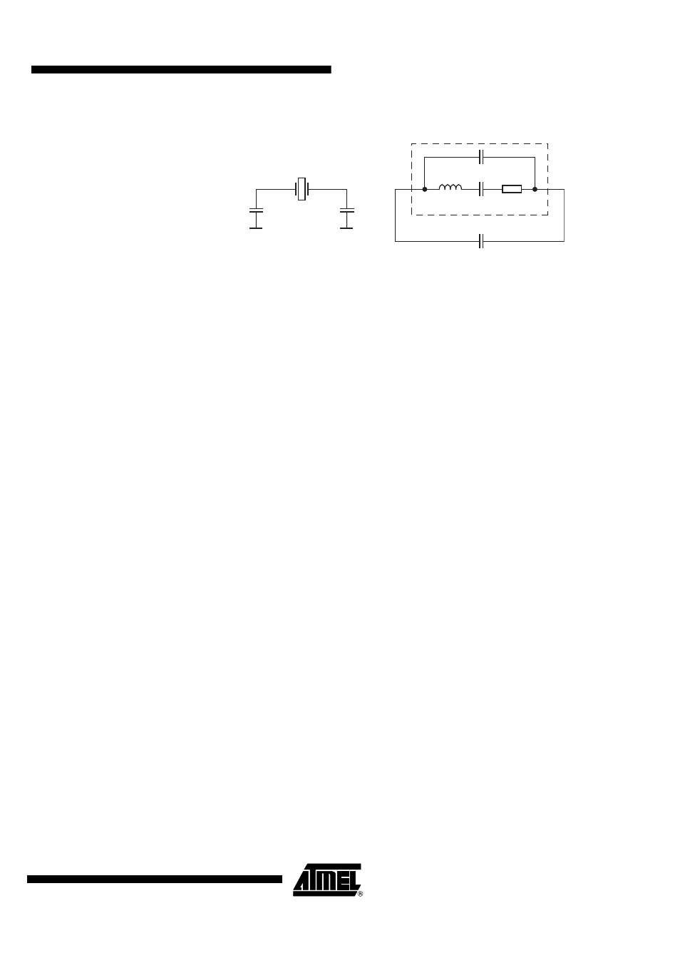
Figure 3-1.
Crystal Equivalent Circuit
With C
m
≤10 fF, C
0
≥ 1.0 pF, C
LN
= 9 pF and C
L1,2
= 16 pF ±1%, the pulling amounts to
P
≤±1 ppm.
The C
0
of the XTAL has to be lower than C
Lmin
/ 2 = 7.9 pF for a Pierce oscillator type in order to
not enter the steep region of pulling versus load capacitance where there is risk of an unstable
oscillation.
To ensure proper start-up behavior, the small signal gain and the negative resistance provided
by this XTO at start is very large. For example, oscillation starts up even in the worst case with a
crystal series resistance of 1.5 k
Ω at C
0
≤2.2 pF with this XTO. The negative resistance is
approximately given by
with Z
1
and Z
2
as complex impedances at pins XTAL1 and XTAL2, hence
Z
1
= –j / (2
× p × f
XTO
× C
L1
) + 5
Ω and Z
2
= –j / (2
× p × f
XTO
× C
L2
) + 5
Ω.
Z
3
consists of crystal C
0
in parallel with an internal 110-k
Ω resistor, hence
Z
3
= –j / (2
× p × f
XTO
× C
0
) / 110 k
Ω, gm is the internal transconductance between XTAL1 and
XTAL2, with typically 20 mS at 25°C.
With f
XTO
= 13.5 MHz, gm = 20 mS, C
L
= 9 pF, and C
0
= 2.2 pF, this results in a negative resis-
tance of about 2 k
Ω. The worst case for technology, supply voltage, and temperature variations
is then always higher than 1.4 k
Ω for C
0
≤2.2 pF.
Due to the large gain at start, the XTO is able to meet a very low start-up time. The oscillation
start-up time can be estimated with the time constant
τ .
After 10
τ to 20τ , an amplitude detector detects the oscillation amplitude and sets XTO_OK to
High if the amplitude is large enough; this activates the CLK_OUT output if it is enabled via the
pins CLK_OUT_CTRL0 and CLK_OUT_CTRL1. Note that the necessary conditions of the
DVCC voltage also have to be fulfilled.
It is recommended to use a crystal with C
m
= 3.0 fF to 10 fF, C
LN
= 9 pF, R
m
< 120
Ω and
C
0
= 1.0 pF to 2.2 pF.
C
0
C
L2
C
L1
C
m
L
m
R
m
C
L
= C
L1
× C
L2
/ (C
L1
+ C
L2
)
XTAL
Crystal Equivalent Circuit
Re Zxtocore
{
} Re
Z
1
Z
3
Z
2
Z
3
Z
1
Z
3
gm
Ч
Ч
+
Ч
+
Ч
Z
1
Z
2
Z
3
Z
1
Z
2
gm
Ч
Ч
+
+
+
-----------------------------------------------------------------------------------------
⎩
⎭
⎨
⎬
⎧
⎫
=
τ
2
4
π
2
f
XTAL
2
C
m
Re Z
xtocore
(
) R
m
+
(
)
Ч
Ч
Ч
Ч
-------------------------------------------------------------------------------------------------------------------
=