Applications information, Package information – Rainbow Electronics DS1842A User Manual
Page 6
The mirror output is typically connected to an ADC
using a resistor to convert the mirrored current into a
voltage. The resistor to ground should be selected such
that the maximum full-scale voltage of the ADC is
reached when the maximum mirrored current is
reached. For example, if the maximum monitored cur-
rent through the APD is 2mA with a 1V ADC full scale,
and the 10:1 mirror is used, then the correct resistor is
approximately 5k
Ω. If both MIR1 and MIR2 are con-
nected together, the correct resistor is 1.6k
Ω.
The mirror response time is dominated by the amount of
capacitance placed on the output. For burst-mode Rx
systems where the fastest response times are required
(approximately a 50ns time constant), a 3.3pF capacitor
and external op amp should be used to buffer the signal
sent to the ADC. For continuous mode applications, a
10nF capacitor is all that is required on the output.
Current Clamp
The DS1842A has a current clamping circuit to protect
the APD by limiting the amount of current from MIROUT.
There are three methods of current clamping available:
1) Internally Defined Current Limit
The device’s current clamp circuit automatically
clamps the current when it exceeds the maximum
MIROUT current.
2) External Shutdown Signal
The CLAMP pin can completely shut down the current
from MIROUT. The CLAMP pin is active high.
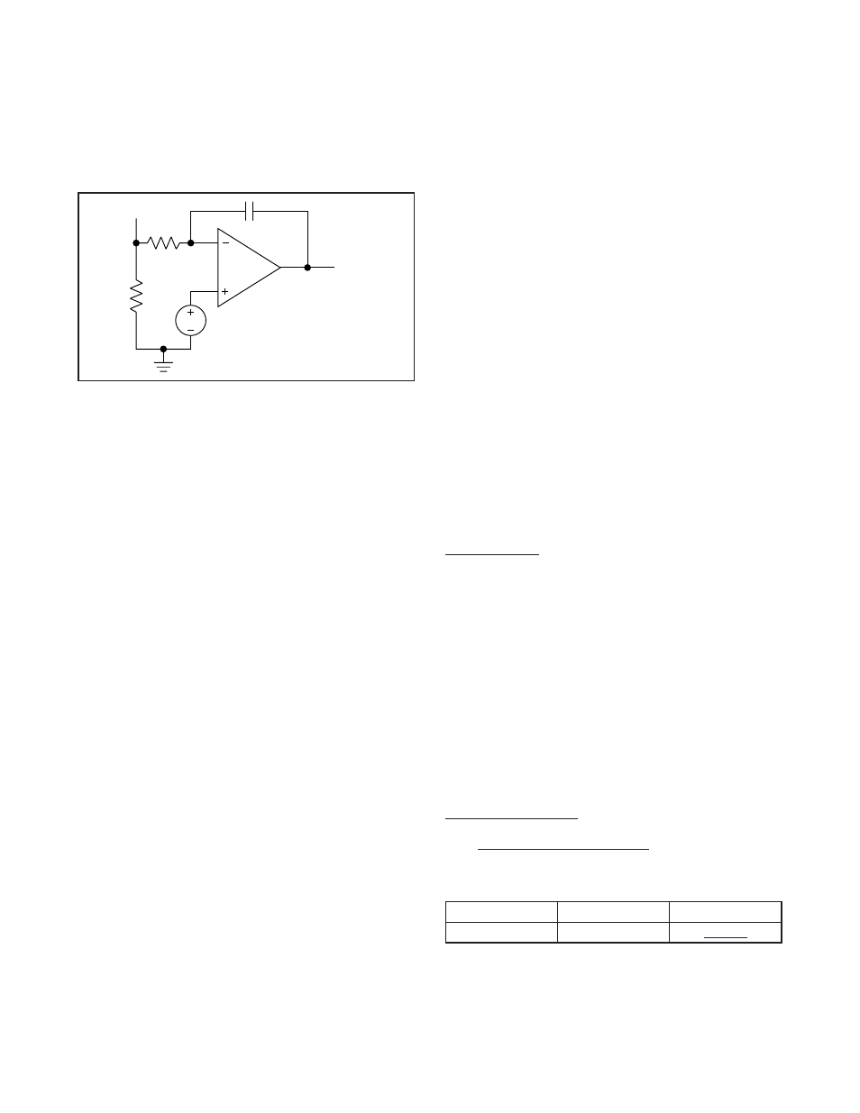
3) Precise Level Set by External Feedback Circuit
A feedback circuit is used to control the level applied to
the CLAMP pin. Figure 1 shows an example feedback
circuit.
Thermal Shutdown
As a safety feature, the DS1842A has a thermal-shut-
down circuit that turns off the MIROUT and MIRIN cur-
rents when the internal die temperature exceeds
T
SHDN
. These currents resume after the device has
cooled.
Switch FET
The DS1842A switching FET is designed to comple-
ment the DS1875 controller’s built-in DC-DC boost con-
troller. APD biasing of 16V to 76V can be achieved
using the DS1842A.
Precision Voltage-Divider
The DS1842A includes a resistor-divider to use as the
feedback network for the boost converter. The
DS1842A resistor-divider ratio, K
R
(R
1
/R
2
), is tightly
controlled, allowing the boost converter output to be set
with very high precision. K
R
can pair with the DS1875’s
internal DC-DC boost controller. K
R
can also be easily
modified by adding external series/parallel resistors;
however, the temperature coefficient of the external
resistors must be considered.
Applications Information
Layout Considerations
Proper PCB layout helps reduce switching noise in the
system. PGND is the connection of the switching FET
and thus carries high current pulses. PGND should also
be connected to the boost converter’s input capacitor
and output bulk capacitor. Ensure that the PGND trace
is low impedance and able to carry the high current
from the FET. To keep the switching noise on PGND
isolated from GND, a star ground configuration should
be used. PGND and GND should only be connected
together at one point on the PCB. This point can be
either the ground side of the output bulk capacitor or
the common ground point of the PCB. Keeping all PCB
traces as short as possible reduces radiated noise,
stray capacitance, and trace resistance.
Package Information
For the latest package outline information and land patterns,
go to
www.maxim-ic.com/packages
. Note that a “+”, “#”, or
“-” in the package code indicates RoHS status only. Package
drawings may show a different suffix character, but the drawing
pertains to the package regardless of RoHS status.
DS1842A
76V, APD, Bias Output Stage with
Current Monitoring
Maxim cannot assume responsibility for use of any circuitry other than circuitry entirely embodied in a Maxim product. No circuit patent licenses are
implied. Maxim reserves the right to change the circuitry and specifications without notice at any time.
6 _____________________Maxim Integrated Products, 120 San Gabriel Drive, Sunnyvale, CA 94086 408-737-7600
© 2009 Maxim Integrated Products
Maxim is a registered trademark of Maxim Integrated Products, Inc.
CLAMP
MIR1
REF
Figure 1. Current Clamp from Current Feedback
PACKAGE TYPE
PACKAGE CODE
DOCUMENT NO.
14 TDFN-EP
T1433+2