Rainbow Electronics DS1842A User Manual
Page 2
DS1842A
76V, APD, Bias Output Stage with
Current Monitoring
2
_______________________________________________________________________________________
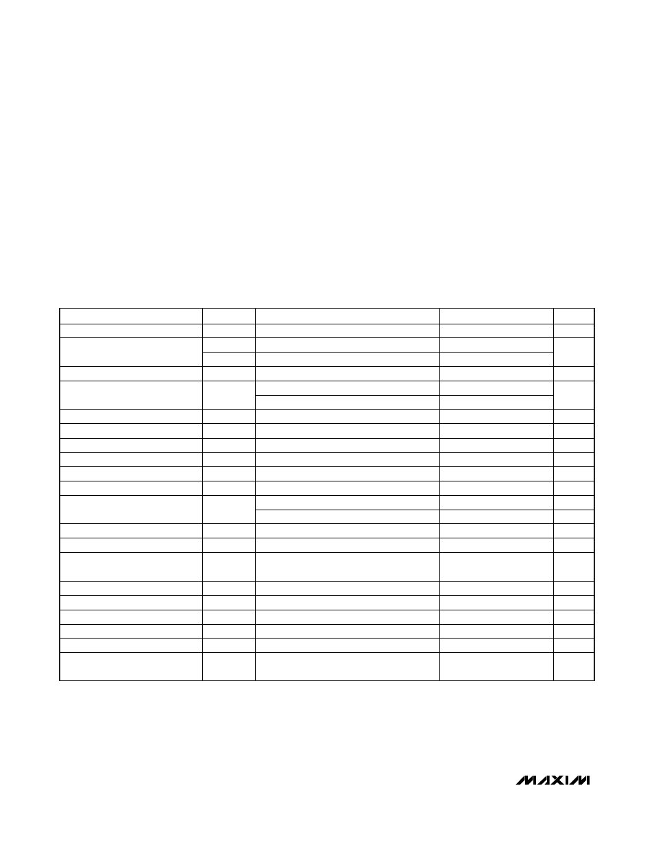
ABSOLUTE MAXIMUM RATINGS
ELECTRICAL CHARACTERISTICS
(T
A
= -40°C to +85°C, unless otherwise noted.)
Stresses beyond those listed under “Absolute Maximum Ratings” may cause permanent damage to the device. These are stress ratings only, and functional
operation of the device at these or any other conditions beyond those indicated in the operational sections of the specifications is not implied. Exposure to
absolute maximum rating conditions for extended periods may affect device reliability.
Note 1: Rising MIROUT transition from 10µA to 1mA; V
MIRIN
= 40V, 2.5k
Ω load.
Note 2: Not production tested. Guaranteed by design.
Voltage Range on GATE and CLAMP
Relative to GND...................................................-0.3V to +12V
Voltage Range on MIRIN, MIROUT, FBIN
MIR1, and MIR2 Relative to GND........................-0.3V to +80V
Voltage Range on FBOUT Relative to GND ..........-0.3V to +6.0V
Voltage Range on LX Relative to GND...................-0.3V to +85V
Operating Junction Temperature Range ...........-40°C to +150°C
Storage Temperature Range .............................-55°C to +135°C
Soldering Temperature ..........................Refer to the IPC JEDEC
J-STD-020 Specification.
PARAMETER SYMBOL
CONDITIONS
MIN
TYP
MAX
UNITS
Switching Frequency
f
SW
0
1.2
MHz
C
GATE
V
GS
= 0V, V
DS
=
25V
40
FET Capacitance
C
LX
f
SW
=
1MHz
90
pF
FET Gate Resistance
R
G
22
V
GS
= 3V, I
D
= 170mA
1
2
FET On-Resistance
R
DSON
V
GS
= 10V, I
D
= 170mA
0.75
1.4
GATE Voltage
V
GS
0
11
V
Switching Current
I
LX
Duty cycle = 10%, f
SW
= 100kHz
680
mA
LX Voltage
V
LX
80
V
LX Leakage
I
IL(LX)
V
GATE
= 0V, V
LX
= 76V
-1
+1
μA
CLAMP Voltage
V
CLAMP
0
11
V
CLAMP Threshold
V
CLT
1.25 1.8 2.35 V
CLAMP = low
1.8
2.75
3.85
mA
Maximum MIROUT Current
I
MIROUT
CLAMP = high
10
μA
MIR1 to MIROUT Ratio
K
MIR1
15V < V
MIRIN
< 76V, I
MIROUT
> 1μA
0.096
0.100
0.104
A/A
MIR2 to MIROUT Ratio
K
MIR2
15V < V
MIRIN
< 76V, I
MIROUT
> 1μA
0.192
0.200
0.208
A/A
MIR1, MIR2 Rise Time
(20%/80%)
t
RC
(Note
1)
30 ns
Shutdown Temperature
T
SHDN
(Note
2)
+150 °C
Hysteresis Temperature
T
HYS
(Note
2)
5 °C
Leakage on GATE and CLAMP
I
IL
-1
+1 μA
Resistor-Divider Ratio (R
1
/R
2
) K
R
T
A
= +25°C, V
FBIN
= 76V
59.5
60.25
Resistor-Divider Tempco
±50
ppm/°C
Resistor-Divider End-to-End
Resistance
R
RES
T
A
= +25°C, V
FBIN
=
76V
308 385 481 k