Port c schematics, Port d – Rainbow Electronics AT90S8515 User Manual
Page 72
72
AT90S8515
0841G–09/01
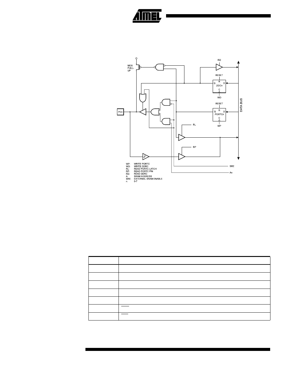
Port C Schematics
Note that all port pins are synchronized. The synchronization latch is, however, not
shown in the figure.
Figure 52. Port C Schematic Diagram (Pins PC0 - PC7)
Port D
Port D is an 8-bit bi-directional I/O port with internal pull-up resistors.
Three I/O memory address locations are allocated for the Port D, one each for the Data
Register – PORTD, $12($32), Data Direction Register – DDRD, $11($31) and the Port D
Input Pins – PIND, $10($30). The Port D Input Pins address is read-only, while the Data
Register and the Data Direction Register are read/write.
The Port D output buffers can sink 20 mA. As inputs, Port D pins that are externally
pulled low will source current if the pull-up resistors are activated.
Some Port D pins have alternate functions as shown in Table 23.
When the pins are used for the alternate function, the DDRD and PORTD registers have
to be set according to the alternate function description.
Table 23. Port D Pin Alternate Functions
Port Pin
Alternate Function
PD0
RXD (UART Input Line)
PD1
TXD (UART Output Line)
PD2
INT0 (External interrupt 0 Input)
PD3
INT1 (External interrupt 1 Input)
PD5
OC1A (Timer/Counter1 Output CompareA Match Output)
PD6
WR
(Write Strobe to External Memory)
PD7
RD
(Read Strobe to External Memory)