Timer/counter1 in pwm mode – Rainbow Electronics AT90S8515 User Manual
Page 40
40
AT90S8515
0841G–09/01
The TEMP register is also used when accessing TCNT1, OCR1A and OCR1B. If the
main program and interrupt routines perform access to registers using TEMP, interrupts
must be disabled during access from the main program (and from interrupt routines if
interrupts are allowed from within interrupt routines).
Timer/Counter1 in PWM Mode
When the PWM mode is selected, Timer/Counter1, the Output Compare Register1A
(OCR1A) and the Output Compare Register1B (OCR1B) form a dual 8-, 9- or 10-bit,
free-running, glitch-free and phase-correct PWM with outputs on the PD5(OC1A) and
OC1B pins. Timer/Counter1 acts as an up/down counter, counting up from $0000 to
TOP (see Table 11), where it turns and counts down again to zero before the cycle is
repeated. When the counter value matches the contents of the 10 least significant bits of
OCR1A or OCR1B, the PD5(OC1A)/OC1B pins are set or cleared according to the set-
tings of the COM1A1/COM1A0 or COM1B1/COM1B0 bits in the Timer/Counter1 Control
Register (TCCR1A). Refer to Table 12 for details.
Note:
X = A or B
Note that in the PWM mode, the 10 least significant OCR1A/OCR1B bits, when written,
are transferred to a temporary location. They are latched when Timer/Counter1 reaches
the value TOP. This prevents the occurrence of odd-length PWM pulses (glitches) in the
event of an unsynchronized OCR1A/OCR1B write. See Figure 32 for an example.
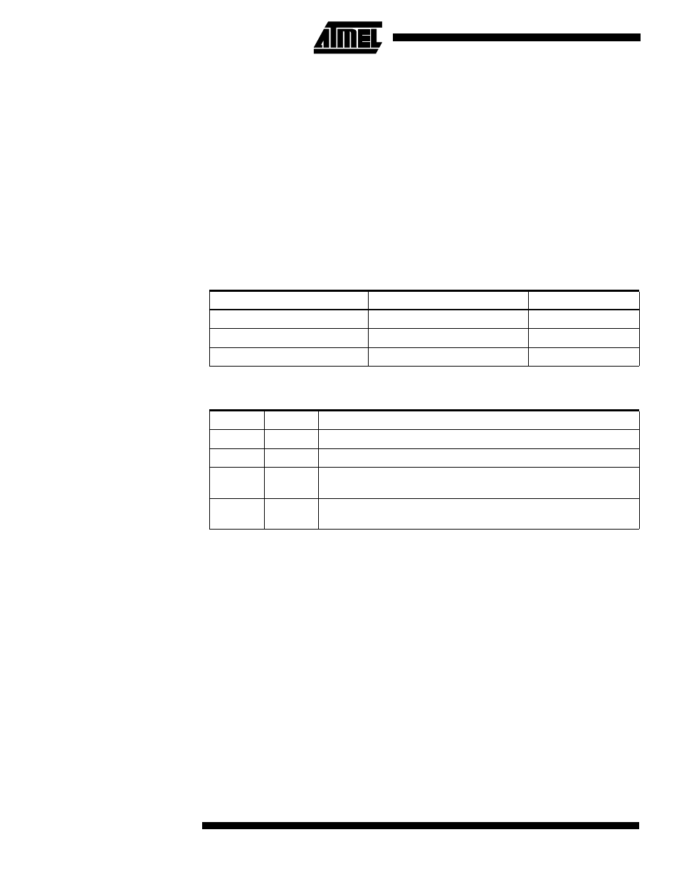
Table 11. Timer TOP Values and PWM Frequency
PWM Resolution
Timer TOP Value
Frequency
8-bit
$00FF (255)
f
TCK1
/510
9-bit
$01FF (511)
f
TCK1
/1022
10-bit
$03FF(1023)
f
TCK1
/2046
Table 12. Compare1 Mode Select in PWM Mode
COM1X1
COM1X0
Effect on OCX1
0
0
Not connected
0
1
Not connected
1
0
Cleared on compare match, up-counting. Set on compare match,
down-counting (non-inverted PWM).
1
1
Cleared on compare match, down-counting. Set on compare match,
up-counting (inverted PWM).