Timer/counter1 – tcnt1h and tcnt1l – Rainbow Electronics AT90S8515 User Manual
Page 38
38
AT90S8515
0841G–09/01
The Stop condition provides a Timer Enable/Disable function. The CK down divided
modes are scaled directly from the CK oscillator clock. If the external pin modes are
used for Timer/Counter1, transitions on PB1/(T1) will clock the counter even if the pin is
configured as an output. This feature can give the user software control of the counting.
Timer/Counter1 – TCNT1H
AND TCNT1L
This 16-bit register contains the prescaled value of the 16-bit Timer/Counter1. To
ensure that both the high and low bytes are read and written simultaneously when the
C P U a c c e s s e s t h e s e r e g i s t e r s , t h e a c c e s s i s p e r f o r m e d u s i n g a n 8 - b i t
temporary register (TEMP). This temporary register is also used when accessing
OCR1A, OCR1B and ICR1. If the main program and interrupt routines perform access
to registers using TEMP, interrupts must be disabled during access from the main pro-
gram (and from interrupt routines if interrupts are allowed from within interrupt routines).
•
TCNT1 Timer/Counter1 Write:
When the CPU writes to the high byte TCNT1H, the written data is placed in the
TEMP register. Next, when the CPU writes the low byte TCNT1L, this byte of data is
combined with the byte data in the TEMP register, and all 16 bits are written to the
TCNT1 Timer/Counter1 register simultaneously. Consequently, the high byte
TCNT1H must be accessed first for a full 16-bit register write operation.
•
TCNT1 Timer/Counter1 Read:
When the CPU reads the low byte TCNT1L, the data of the low byte TCNT1L is sent
to the CPU and the data of the high byte TCNT1H is placed in the TEMP register.
When the CPU reads the data in the high byte TCNT1H, the CPU receives the data
in the TEMP register. Consequently, the low byte TCNT1L must be accessed first for
a full 16-bit register read operation.
The Timer/Counter1 is realized as an up or up/down (in PWM mode) counter with read
and write access. If Timer/Counter1 is written to and a clock source is selected, the
Timer/Counter1 continues counting in the timer clock cycle after it is preset with the writ-
ten value.
Timer/Counter1 Output
Compare Register – OCR1AH
AND OCR1AL
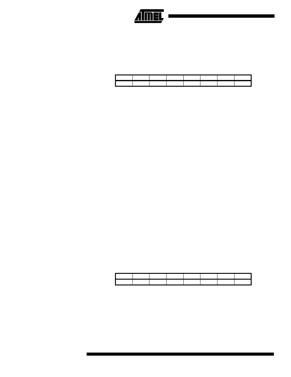
Bit
15
14
13
12
11
10
9
8
$2D ($4D)
MSB
TCNT1H
$2C ($4C)
LSB
TCNT1L
7
6
5
4
3
2
1
0
Read/Write
R/W
R/W
R/W
R/W
R/W
R/W
R/W
R/W
R/W
R/W
R/W
R/W
R/W
R/W
R/W
R/W
Initial Value
0
0
0
0
0
0
0
0
0
0
0
0
0
0
0
0
Bit
15
14
13
12
11
10
9
8
$2B ($4B)
MSB
OCR1AH
$2A ($4A)
LSB
OCR1AL
7
6
5
4
3
2
1
0
Read/Write
R/W
R/W
R/W
R/W
R/W
R/W
R/W
R/W
R/W
R/W
R/W
R/W
R/W
R/W
R/W
R/W
Initial Value
0
0
0
0
0
0
0
0
0
0
0
0
0
0
0
0