Data modes, Spi control register – spcr – Rainbow Electronics AT90S8515 User Manual
Page 49
49
AT90S8515
0841G–09/01
pins are inputs. When SS is driven high, all pins are inputs and the SPI is passive, which
means that it will not receive incoming data. Note that the SPI logic will be reset once
the SS pin is brought high. If the SS pin is brought high during a transmission, the SPI
will stop sending and receiving immediately and both data received and data sent must
be considered as lost.
Data Modes
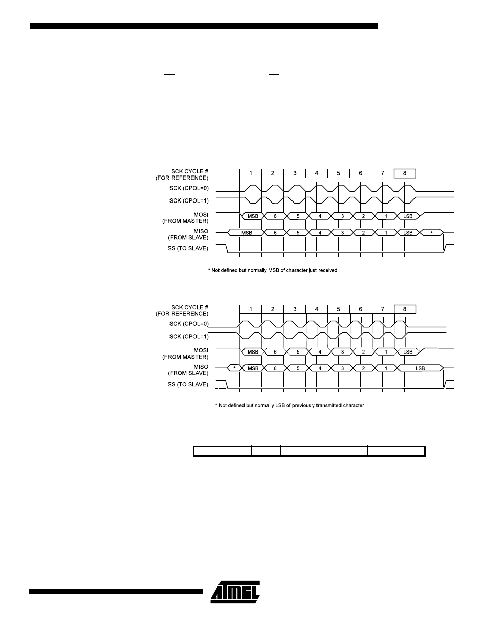
There are four combinations of SCK phase and polarity with respect to serial data,
which are determined by control bits CPHA and CPOL. The SPI data transfer formats
are shown in Figure 36 and Figure 37.
Figure 36. SPI Transfer Format with CPHA = 0 and DORD = 0
Figure 37. SPI Transfer Format with CPHA = 1 and DORD = 0
SPI Control Register – SPCR
• Bit 7 – SPIE: SPI Interrupt Enable
This bit causes the SPI interrupt to be executed if SPIF bit in the SPSR register is set
and the global interrupts are enabled.
• Bit 6 – SPE: SPI Enable
When the SPE bit is set (one), the SPI is enabled. This bit must be set to enable any SPI
operations.
Bit
7
6
5
4
3
2
1
0
$0D ($2D)
SPIE
SPE
DORD
MSTR
CPOL
CPHA
SPR1
SPR0
SPCR
Read/Write
R/W
R/W
R/W
R/W
R/W
R/W
R/W
R/W
Initial Value
0
0
0
0
0
0
0
0