Sram data memory – internal and external – Rainbow Electronics AT90S8515 User Manual
Page 12
12
AT90S8515
0841G–09/01
SRAM Data Memory –
Internal and External
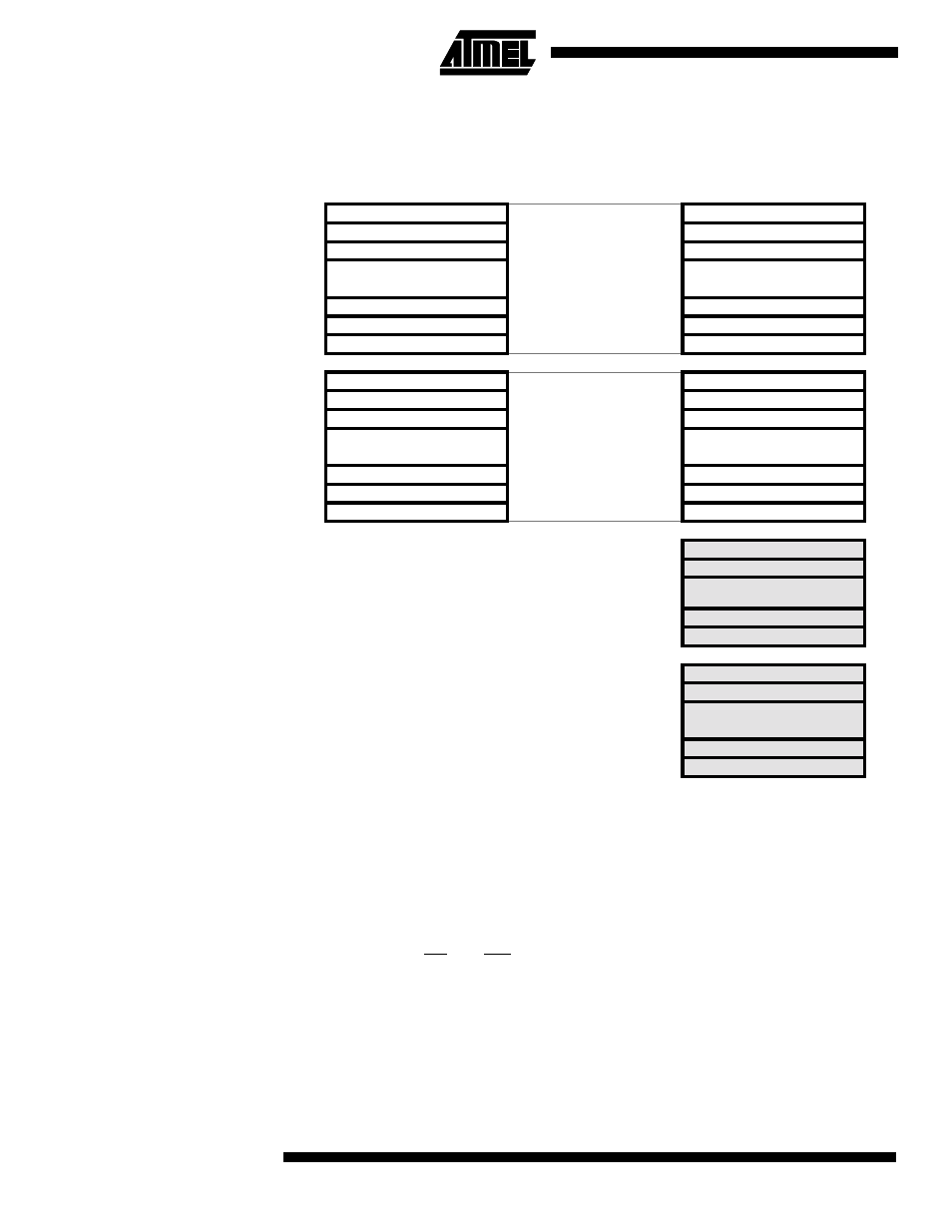
Figure 8 shows how the AT90S8515 SRAM memory is organized.
Figure 8. SRAM Organization
The lower 608 data memory locations address the Register file, the I/O memory and the
internal data SRAM. The first 96 locations address the Register file + I/O memory, and
the next 512 locations address the internal data SRAM. An optional external data SRAM
can be placed in the same SRAM memory space. This SRAM will occupy the location
following the internal SRAM and up to as much as 64K - 1, depending on SRAM size.
When the addresses accessing the data memory space exceed the internal data SRAM
locations, the external data SRAM is accessed using the same instructions as for the
internal data SRAM access. When the internal data space is accessed, the read and
write strobe pins (RD and WR) are inactive during the whole access cycle. External
SRAM operation is enabled by setting the SRE bit in the MCUCR register. See page 29
for details.
Accessing external SRAM takes one additional clock cycle per byte compared to access
of the internal SRAM. This means that the commands LD, ST, LDS, STS, PUSH and
POP take one additional clock cycle. If the stack is placed in external SRAM, interrupts,
subroutine calls and returns take two clock cycles extra because the 2-byte program
counter is pushed and popped. When external SRAM interface is used with wait state,
Register File
Data Address Space
R0
$0000
R1
$0001
R2
$0002
…
…
R29
$001D
R30
$001E
R31
$001F
I/O Registers
$00
$0020
$01
$0021
$02
$0022
…
…
$3D
$005D
$3E
$005E
$3F
$005F
Internal SRAM
$0060
$0061
…
$025E
$025F
External SRAM
$0260
$0261
…
$FFFE
$FFFF