Port c, Port c data register – portc, Figure 51. port b schematic diagram (pin pb7) – Rainbow Electronics AT90S8515 User Manual
Page 70
70
AT90S8515
0841G–09/01
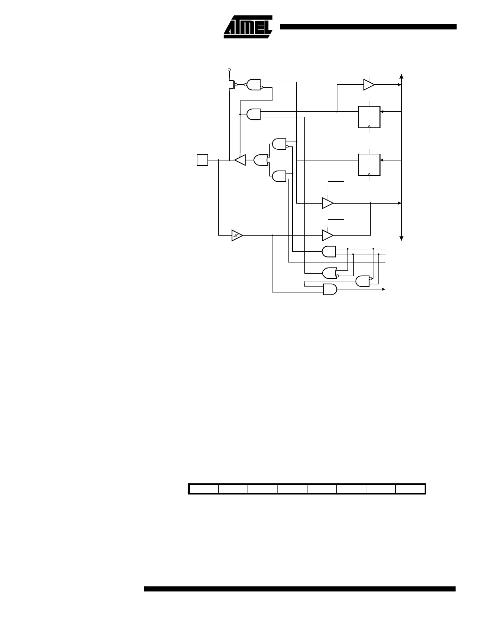
Figure 51. Port B Schematic Diagram (Pin PB7)
Port C
Port C is an 8-bit bi-directional I/O port. Three I/O memory address locations are allo-
cated for the Port C, one each for the Data Register – PORTC, $15($35), Data Direction
Register – DDRC, $14($34) and the Port C Input Pins – PINC, $13($33). The Port C
Input Pins address is read-only, while the Data Register and the Data Direction Register
are read/write.
All port pins have individually selectable pull-up resistors. The Port C output buffers can
sink 20 mA and thus drive LED displays directly. When pins PC0 to PC7 are used as
inputs and are externally pulled low, they will source current if the internal pull-up resis-
tors are activated.
The Port C pins have alternate functions related to the optional external data SRAM.
Port C can be configured to be the high-order address byte during accesses to external
data memory. When Port C is set to the alternate function by the SRE (external SRAM
enable) bit in the MCUCR (MCU Control Register), the alternate settings override the
Data Direction Register.
Port C Data Register – PORTC
DA
T
A
BUS
D
D
Q
Q
RESET
RESET
C
C
WD
WP
RD
MOS
PULL-
UP
PB7
R
R
WP:
WD:
RL:
RP:
RD:
SPE:
MSTR
WRITE PORTB
WRITE DDRB
READ PORTB LATCH
READ PORTB PIN
READ DDRB
SPI ENABLE
MASTER SELECT
DDB7
PORTB7
SPE
MSTR
SPI CLOCK
OUT
SPI CLOCK
IN
RL
RP
Bit
7
6
5
4
3
2
1
0
$15 ($35)
PORTC7
PORTC6
PORTC5
PORTC4
PORTC3
PORTC2
PORTC1
PORTC0
PORTC
Read/Write
R/W
R/W
R/W
R/W
R/W
R/W
R/W
R/W
Initial Value
0
0
0
0
0
0
0
0