Rainbow Electronics AT90S8515 User Manual
Page 54

54
AT90S8515
0841G–09/01
The receiver front-end logic samples the signal on the RXD pin at a frequency 16 times
the baud rate. While the line is idle, one single sample of logical “0” will be interpreted as
the falling edge of a start bit and the start bit detection sequence is initiated. Let sample
1 denote the first zero-sample. Following the 1-to-0 transition, the receiver samples the
RXD pin at samples 8, 9 and 10. If two or more of these three samples are found to be
logical “1”s, the start bit is rejected as a noise spike and the receiver starts looking for
the next 1-to-0 transition.
If, however, a valid start bit is detected, sampling of the data bits following the start bit is
performed. These bits are also sampled at samples 8, 9 and 10. The logical value found
in at least two of the three samples is taken as the bit value. All bits are shifted into the
Transmitter Shift register as they are sampled. Sampling of an incoming character is
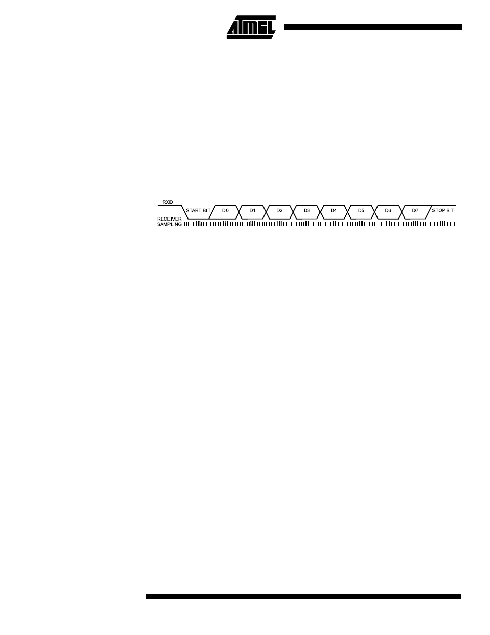
shown in Figure 40.
Figure 40. Sampling Received Data
When the stop bit enters the receiver, the majority of the three samples must be “1” to
accept the stop bit. If two or more samples are logical “0”s, the Framing Error (FE) flag in
the UART Status Register (USR) is set. Before reading the UDR register, the user
should always check the FE bit to detect framing errors.
Whether or not a valid stop bit is detected at the end of a character reception cycle, the
data is transferred to UDR and the RXC flag in USR is set. UDR is in fact two physically
separate registers, one for transmitted data and one for received data. When UDR is
read, the Receive Data register is accessed, and when UDR is written, the Transmit
Data register is accessed. If 9-bit data word is selected (the CHR9 bit in the UART Con-
trol Register, UCR is set), the RXB8 bit in UCR is loaded with bit 9 in the Transmit Shift
register when data is transferred to UDR.
If, after having received a character, the UDR register has not been read since the last
receive, the OverRun (OR) flag in USR is set. This means that the last data byte shifted
into the shift register could not be transferred to UDR and has been lost. The OR bit is
buffered and is updated when the valid data byte in UDR is read. Thus, the user should
always check the OR bit after reading the UDR register in order to detect any overruns if
the baud rate is high or CPU load is high.
When the RXEN bit in the UCR register is cleared (zero), the receiver is disabled. This
means that the PD0 pin can be used as a general I/O pin. When RXEN is set, the UART
Receiver will be connected to PD0, which is forced to be an input pin regardless of the
setting of the DDD0 bit in DDRD. When PD0 is forced to input by the UART, the
PORTD0 bit can still be used to control the pull-up resistor on the pin.
When the CHR9 bit in the UCR register is set, transmitted and received characters are
9 bits long, plus start and stop bits. The ninth data bit to be transmitted is the TXB8 bit in
UCR register. This bit must be set to the wanted value before a transmission is initiated
by writing to the UDR register. The ninth data bit received is the RXB8 bit in the UCR
register.
