Max6948b, Timing characteristics – Rainbow Electronics MAX6948B User Manual
Page 5
High-Efficiency PWM LED Driver with Boost
Converter and Five Constant-Current GPIO Ports
5
MAX6948B
TIMING CHARACTERISTICS
(Typical Application Circuit, V+ = 2.7V to 5.0V, V
DD
= 1.7V to V+, T
A
= T
MIN
to T
MAX
, unless otherwise noted. Typical values are at
V+ = 3.3V, V
DD
= 2.5V, T
A
= +25NC.) (Note 4)
Note 4: All parameters are tested at T
A
= +25NC. Specifications over temperature are guaranteed by design.
Note 5: The DI
PORT_
specifies current matching between ports of a single part.
Note 6: Current matching is defined as the percent error of any individual port from the average current of the maximum value
measured and the minimum value measured. It can be found using the equation DI
PORT_
= 100 x (I
MMAVG
- I
MEAS
)/
I
MMAVG
where I
MMAVG
= (I
MEASMAX
+ I
MEASMIN
)/2.
Note 7: Guaranteed by design.
Note 8: A master device must provide a hold time of at least 300ns for the SDA signal (referred to V
IL
of the SCL signal) to
bridge the undefined region of SCL’s falling edge.
Note 9: I
SINK
P 6mA. C
b
= total capacitance of one bus line in pF. t
R
and t
F
are measured between 0.3 x V
DD
and 0.7 x V
DD
.
Note 10: Input filters on the SDA, SCL, and AD0 inputs suppress noise spikes less than 50ns.
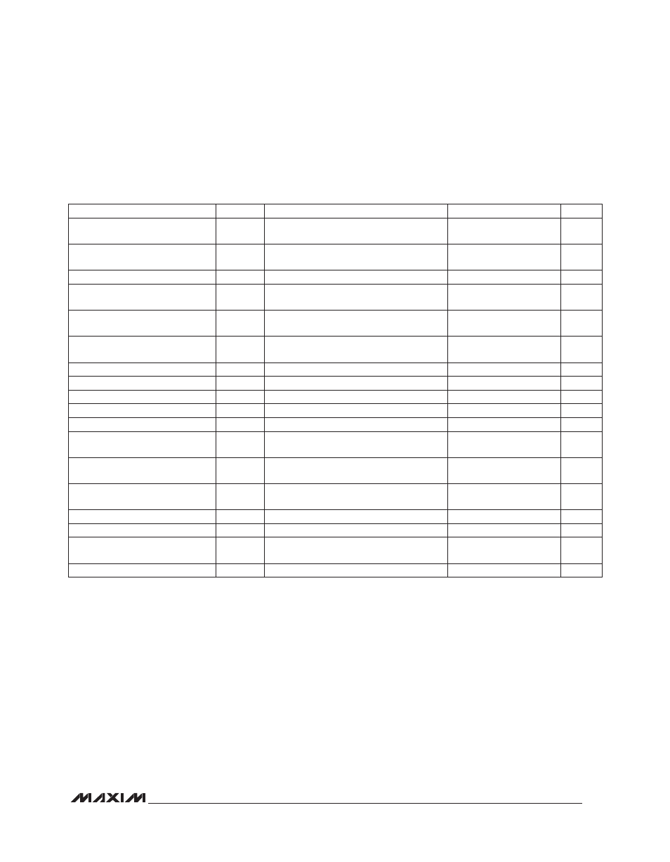
PARAMETER
SYMBOL
CONDITIONS
MIN
TYP
MAX
UNITS
Internal Boost-Converter PWM
Clock Frequency
f
INT_
BOOST
98
125
145
kHz
Internal GPIO PWM Clock
Frequency
f
INT_GPIO
24
31.25
38
kHz
SCL Serial-Clock Frequency
f
SCL
400
kHz
Bus Free Time Between a STOP
and START Condition
t
BUF
1.3
F
s
Hold Time (Repeated) START
Condition
t
HD, STA
0.6
F
s
Repeated START Condition Setup
Time
t
SU, STA
0.6
F
s
STOP Condition Setup Time
t
SU, STO
0.6
F
s
Data Hold Time
t
HD, DAT
(Note 8)
0.9
F
s
Data Setup Time
t
SU, DAT
180
ns
SCL Clock Low Period
t
LOW
1.3
F
s
SCL Clock High Period
t
HIGH
0.7
F
s
Rise Time of Both SDA and SCL
Signals, Receiving
t
R
(Notes 7, 9)
20 +
0.1C
b
300
ns
Fall Time of Both SDA and SCL
Signals, Receiving
t
F
(Notes 7, 9)
20 +
0.1C
b
300
ns
Fall Time of SDA Transmitting
t
F, TX
(Notes 7, 9)
20 +
0.1C
b
250
ns
Pulse Width of Spike Suppressed
t
SP
(Notes 7, 10)
50
ns
Serial Bus Timeout
t
OUT
20
30
50
ms
Capacitive Load for Each Bus
Line
C
b
(Note 7)
400
pF
RST Pulse Width
t
W
1
F
s