Max6948b – Rainbow Electronics MAX6948B User Manual
Page 23
High-Efficiency PWM LED Driver with Boost
Converter and Five Constant-Current GPIO Ports
23
MAX6948B
Figure 11. Acknowledge
Figure 12. Slave Address
Table 13. MAX6948B Slave Address Map
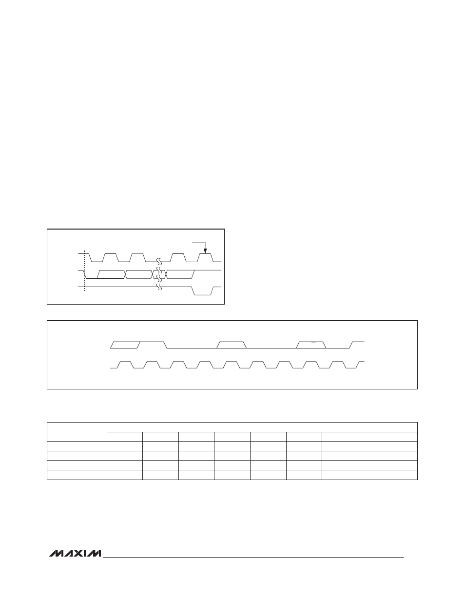
Acknowledge
The acknowledge bit is a clocked 9th bit (Figure 11),
which the recipient uses to handshake receipt of each
byte of data. Thus, each byte transferred effectively
requires 9 bits. The master generates the 9th clock
pulse, and the recipient pulls down SDA during the
acknowledge clock pulse, and therefore the SDA line
is stable-low during the high period of the clock pulse.
When the master is transmitting to the MAX6948B, the
MAX6948B generates the acknowledge bit because
the MAX6948B is the recipient. When the MAX6948B
is transmitting to the master, the master generates the
acknowledge bit because the master is the recipient.
Slave Addresses
The MAX6948B has a 7-bit long slave address (Figure 12).
The bit following a 7-bit slave address is the R/W bit, which
is low for a write command and high for a read command.
Five bits (A6, A5, A4, A2, and A1), of the MAX6948B
slave address are always 1, 0, 0, 0, and 0, respectively.
Slave address bits A7 and A3 correspond, by the matrix
in Table 13, to the states of the device address input
AD0, and A0 corresponds to the R/W bit. The AD0 input
can be connected to any of four signals: GND, V
DD
,
SDA, or SCL, giving four possible slave-address pairs,
allowing up to four MAX6948B devices to share the bus.
Because SDA and SCL are dynamic signals, care must
be taken to ensure that AD0 transitions no sooner than
the signals on SDA and SCL.
The MAX6948B monitors the bus continuously, waiting for
a START condition followed by its slave address. When
the MAX6948B recognizes its slave address, it acknowl-
edges and is then ready for continued communication.
SCL
SDA BY
TRANSMITTER
CLOCK PULSE
FOR ACKNOWLEDGE
START
CONDITION
SDA BY
RECEIVER
1
2
8
9
S
SDA
A7
1
0
0
A3
0
0
R/W
ACK
SCL
MSB
LSB
PIN AD0
DEVICE ADDRESS
A7
A6
A5
A4
A3
A2
A1
A0
GND
0
1
0
0
0
0
0
R/W
V
DD
0
1
0
0
1
0
0
R/W
SCL
1
1
0
0
0
0
0
R/W
SDA
1
1
0
0
1
0
0
R/W