Max6948b, Rst input, Reset-run option – Rainbow Electronics MAX6948B User Manual
Page 21: Cinterface
High-Efficiency PWM LED Driver with Boost
Converter and Five Constant-Current GPIO Ports
21
MAX6948B
RST Input
The active-low RST input operates as a reset that voids
any current I
2
C transaction involving the MAX6948B,
forcing the device into the I
2
C STOP condition. Use the
D6 bit in the configuration register (Table 2) to configure
RST to reset all the internal registers to the power-on-
reset state (Table 3). The RST input is overvoltage toler-
ant to 5.5V.
The MAX6948B ignores all I
2
C bus activity while RST
remains low. The device uses this feature to minimize
supply current in power-critical applications by effective-
ly disconnecting the MAX6948B from the bus during idle
periods. RST also operates as a bus multiplexer, allow-
ing multiple devices to use the same I
2
C slave address.
Drive only one MAX6948B RST input high at any time to
use RST as a bus multiplexer.
The MAX6948B features a reset-run option. Taking the
RST input high brings the driver out of shutdown in addi-
tion to its normal function of enabling the device’s I
2
C
interface.
Reset-Run Option
The MAX6948B features a reset-run option enabling RST
to bring the driver out of shutdown, in addition to its nor-
mal function of enabling the MAX6948B’s I
2
C interface.
This provides an alternative method of bringing the driver
out of shutdown to writing to the configuration register
through the serial interface. The reset-run timing uses the
internal PWM clock.
After enabling the reset-run option, the MAX6948B uses
the rising edge on RST, followed by no I
2
C interface activ-
ity to the MAX6948B for 128 to 129 periods of the GPIO
PWM clock (32kHz typ) to trigger the reset-run option.
If this timeout period elapses without the MAX6948B
acknowledging an I
2
C transaction, the device sets the
run bit (D0) in the configuration register and brings itself
out of shutdown, activating any programmed ramp-up.
If RST pulses high for less than this timeout period to
trigger a reset run, the MAX6948B ignores the pulse and
continues to wait for a suitable trigger.
Cancel the reset-run trigger by transmitting an I
2
C com-
munication to the MAX6948B before the timeout period
elapses. The trigger cancels when the MAX6948B
acknowledges the I
2
C transaction and requires send-
ing at least the MAX6948B’s I
2
C slave address. The
minimum timeout period is equal to 4ms. The minimum
I
2
C clock speed that guarantees a successful start bit
and 8 data bits (9 bits total) within the minimum timeout
period is 9/4ms equal to 2.25kHz. Canceling the reset-
run trigger clears the reset-run bit (D1) in the configura-
tion register, disabling reset run. The run bit (D0) in the
configuration register remains cleared and the driver
remains in shutdown.
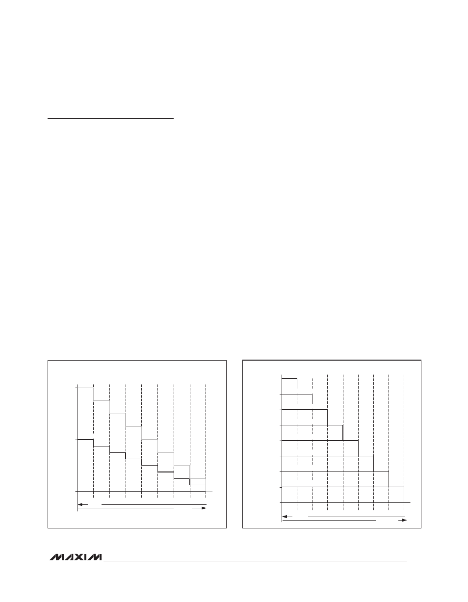
Figure 6. Output Fade DAC (Global Current = 0x07)
Figure 7. Global Current Modifies Ramp-Down Behavior
30mA
10mA
15mA
5mA
0mA
P0, P1
CURRENT
P2, P3, P4
CURRENT
RAMP-UP
FULL
CURRENT
7/8
CURRENT
6/8
CURRENT
5/8
CURRENT
4/8
CURRENT
3/8
CURRENT
2/8
CURRENT
1/8
CURRENT
ZERO
CURRENT
PORT CURRENT = HALF
RAMP-DOWN
PORT CURRENT = FULL
0mA
30mA
22.5mA
15mA
7.5mA
0mA
P0, P1
CURRENT
FULL
CURRENT
7/8
CURRENT
6/8
CURRENT
5/8
CURRENT
4/8
CURRENT
3/8
CURRENT
2/8
CURRENT
1/8
CURRENT
ZERO
CURRENT
26.25mA
18.75mA
11.25mA
3.75mA
10mA
7.5mA
5mA
2.5mA
0mA
P2, P3, P4
CURRENT
8.75mA
6.25mA
3.75mA
1.25mA
RAMP-UP
RAMP-DOWN
GLOBAL CURRENT = 0x07
GLOBAL CURRENT = 0x06
GLOBAL CURRENT = 0x05
GLOBAL CURRENT = 0x04
GLOBAL CURRENT = 0x03
GLOBAL CURRENT = 0x02
GLOBAL CURRENT = 0x01
GLOBAL CURRENT = 0x00