Max6948b, Electrical characteristics, Absolute maximum ratings – Rainbow Electronics MAX6948B User Manual
Page 2
High-Efficiency PWM LED Driver with Boost
Converter and Five Constant-Current GPIO Ports
2
MAX6948B
V+ to GND ...............................................................-0.3V to +6V
V
DD
, COMP to GND ....................................-0.3V to (V+ + 0.3V)
PGND to GND ......................................................-0.3V to +0.3V
LX to PGND (Note 1) .............................................-0.3V to +30V
Current into LX (Note 1) ...................................................700mA
OUT, LEDSW to PGND (Note 1) ...........................-0.3V to +30V
P0–P4 to GND .........................................................-0.3V to +6V
RST, SDA, SCL, AD0 to GND .................. -0.3V to (V
DD
+ 0.3V)
FB to PGND (Note 1) ............................................-0.3V to +0.3V
I.C. to GND ...........................................................-0.3V to +0.3V
DC Current on P0–P4 .........................................................50mA
DC Current on SDA ............................................................10mA
Total GND Current ............................................................150mA
Total PGND Current .........................................................150mA
Continuous Power Dissipation (T
A
= +70NC)
25-Bump WLP (derate 10.8mW/NC above +70NC) ......866mW
Junction-to-Ambient Thermal Resistance (B
JA
) (Note 2)
25-Bump WLP ..............................................................93NC/W
Operating Temperature Range
(T
MIN
to T
MAX
) .............................................. -40NC to +105NC
Junction Temperature .....................................................+150NC
Storage Temperature Range ............................ -65NC to +150NC
ESD Protection
Human Body Model (R
D
= 1.5kI, C
S
= 100pF)
P0–P4, OUT, LEDSW, FB to GND ................................Q8kV
All Other Pins ................................................................Q2kV
Lead Temperature (soldering, 10s)
25-Bump WLP .............................................................(Note 3)
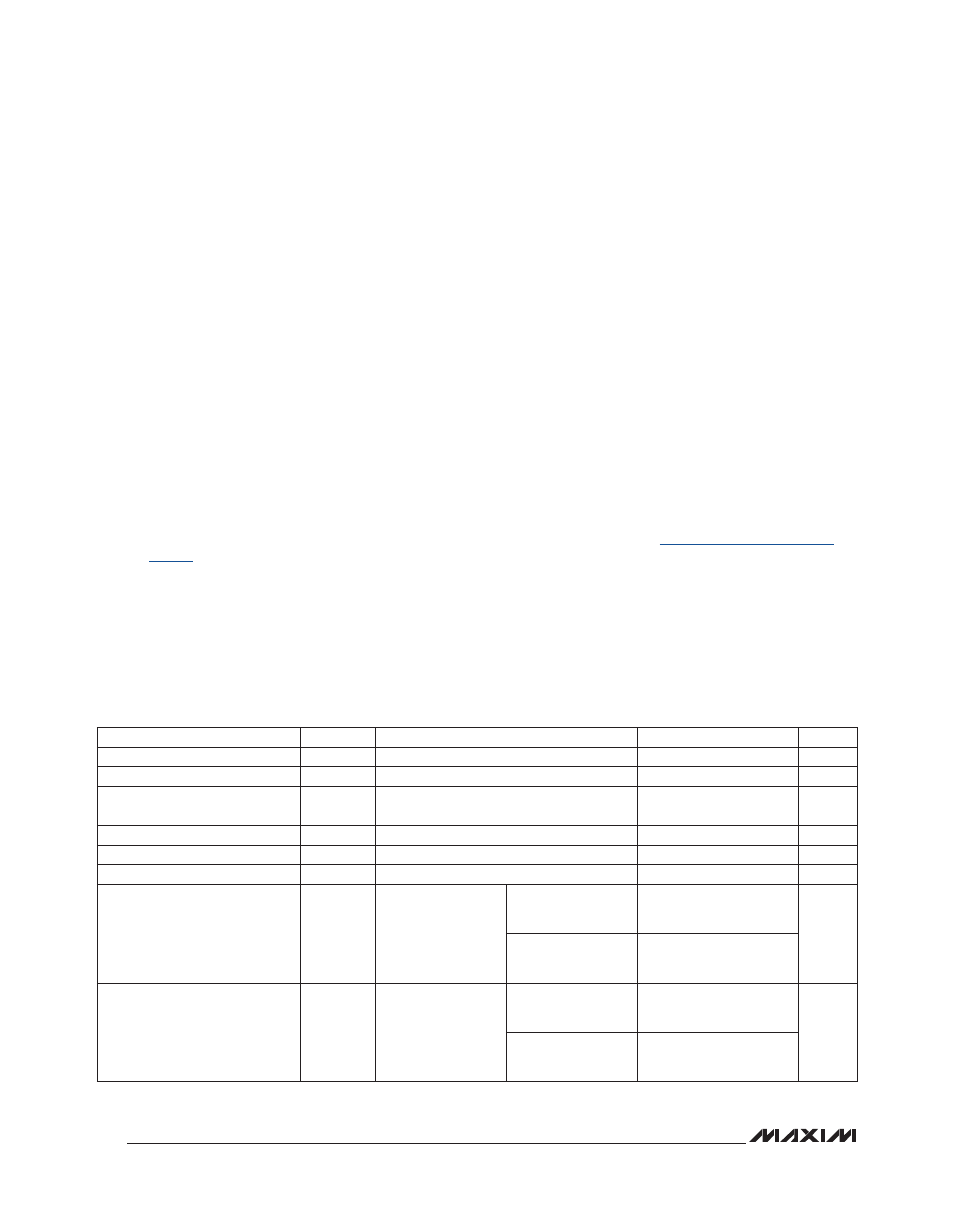
ELECTRICAL CHARACTERISTICS
(Typical Application Circuit, V+ = 2.7V to 5.0V, V
DD
= 1.7V to V+, T
A
= T
MIN
to T
MAX
, unless otherwise noted. Typical values are at
V+ = 3.3V, V
DD
= 2.5V, T
A
= +25NC.) (Note 4)
ABSOLUTE MAXIMUM RATINGS
Stresses beyond those listed under “Absolute Maximum Ratings” may cause permanent damage to the device. These are stress ratings only, and functional opera-
tion of the device at these or any other conditions beyond those indicated in the operational sections of the specifications is not implied. Exposure to absolute
maximum rating conditions for extended periods may affect device reliability.
Note 1: LX, FB, LEDSW pins have an internal clamp diode to PGND. Applications that forward bias these diodes should take care
not to exceed the power dissipation limits of the device.
Note 2: Package thermal resistances were obtained using the method described in JEDEC specification JESD51-7, using a
single-layer board. For detailed information on package thermal considerations, refer to
Note 3: Refer to the Pb-free solder reflow requirement in J-STD -020, Rev D.1.
PARAMETER
SYMBOL
CONDITIONS
MIN
TYP
MAX
UNITS
Operating Supply Voltage (V+)
V+
2.7
3.3
5.0
V
Operating Supply Voltage (V
DD
)
V
DD
1.7
2.5
V+
V
Output Load External Supply
Voltage
V
OUT
Boost-converter output
28
V
Port External Supply Voltage
V
EXT
P0–P4 at high impedance
5.5
V
Port Voltage (P0, P4)
V
PORT
Constant-current on
V+
V
Power-On-Reset Voltage
V
POR
Voltage rising
1.7
V
Standby Current
I
STBY
Standby mode,
boost converter off,
RST = V
DD
, all digi-
tal inputs at V
DD
or
GND
T
A
= +25NC
1.5
4
F
A
T
A
= T
MIN
to T
MAX
6
Standby Current in Reset
(Interface Active)
I
RST
Standby mode,
RST = GND,
f
SCL
= 400kHz, all
other digital inputs
at V
DD
or GND
T
A
= +25NC
1.6
4
F
A
T
A
= T
MIN
to T
MAX
6