Max6948b, Boost converter – Rainbow Electronics MAX6948B User Manual
Page 12
High-Efficiency PWM LED Driver with Boost
Converter and Five Constant-Current GPIO Ports
12
MAX6948B
Boost Converter
Boost-Converter Output PWM
The MAX6948B boost converter has 10-bit PWM opera-
tion using an internal 125kHz clock. This yields a PWM
period of 1024/125k = 8.192ms. PWM operation allows
the user to adjust the LED intensity and lower the average
current by enabling and disabling the boost converter at
a selectable rate. This rate is set using the boost-con-
verter output PWM registers (Tables 4, 5). The duty cycle
ranges from 0/1024 (no intensity or off) to 1023/1024 (full
intensity). Eight of the 10 bits, which include the MSB, are
in a single register (0x20) to allow a single I
2
C write to
set the majority of the intensity level and minimize visible
flicker during intensity changes. The LSB register (0x21)
allows for very fine adjustments in LED intensity.
Boost-Converter Status Register
The MAX6948B checks the boost converter and indi-
cates its status in the boost-converter status register
(Table 6). Faults indicated in this register include ther-
mal shutdown, overvoltage, and current limit. The boost
converter goes into standby mode whenever the boost
standby bit (D0) = 1.
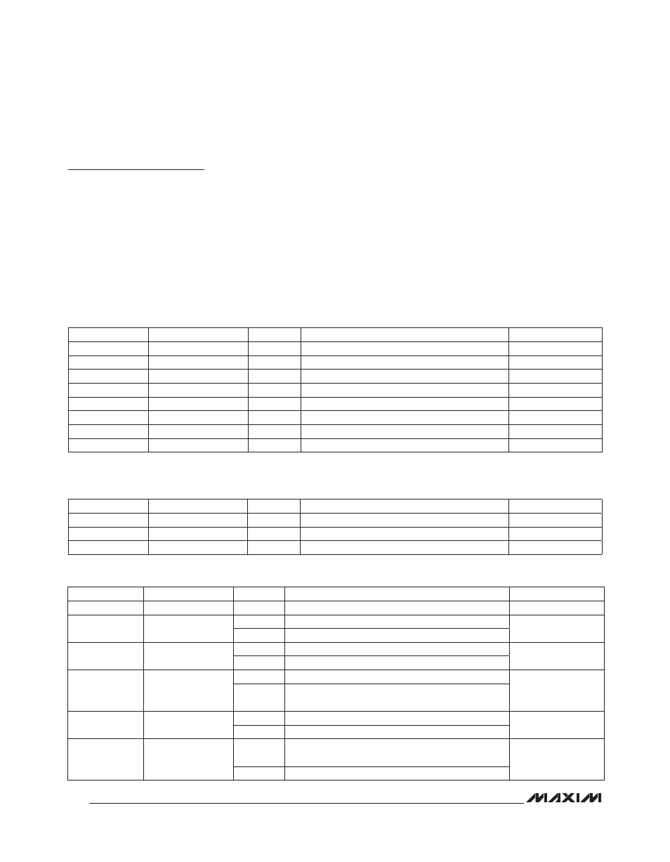
Table 4. Boost-Converter Output PWM (MSB) Register Format (0x20)
Table 5. Boost-Converter Output PWM (LSB) Register Format (0x21)
Table 6. Boost-Converter Status Register Format (0x22)
X = Don’t care.
REGISTER BIT
DESCRIPTION
VALUE
FUNCTION
DEFAULT VALUE
D7
Bit 9
—
Boost-converter output PWM bit 9 (MSB)
0
D6
Bit 8
—
Boost-converter output PWM bit 8
0
D5
Bit 7
—
Boost-converter output PWM bit 7
0
D4
Bit 6
—
Boost-converter output PWM bit 6
0
D3
Bit 5
—
Boost-converter output PWM bit 5
0
D2
Bit 4
—
Boost-converter output PWM bit 4
0
D1
Bit 3
—
Boost-converter output PWM bit 3
0
D0
Bit 2
—
Boost-converter output PWM bit 2
0
REGISTER BIT
DESCRIPTION
VALUE
FUNCTION
DEFAULT VALUE
D7–D2
Reserved
000000
—
000000
D1
Bit 1
—
Boost-converter output PWM bit 1
0
D0
Bit 0
—
Boost-converter output PWM bit 0 (LSB)
0
REGISTER BIT
DESCRIPTION
VALUE
FUNCTION
DEFAULT VALUE
D7, D6, D5
Reserved
000
—
000
D4
Schottky open
0
Schottky diode present
Read only
1
Schottky diode open
D3
Current limit
0
Normal output current
Read only
1
Converter output current exceeded the current limit
D2
Thermal shutdown
0
Normal operation
Read only
1
Device temperature has exceeded thermal
shutdown threshold
D1
Overvoltage
0
Normal operation
Read only
1
V
OUT
exceeded overvoltage limit
D0
Boost standby
0
Boost converter operating according to PWM
register and configuration register
1
1
Boost converter in standby mode