Max6948b, Electrical characteristics (continued) – Rainbow Electronics MAX6948B User Manual
Page 4
High-Efficiency PWM LED Driver with Boost
Converter and Five Constant-Current GPIO Ports
4
MAX6948B
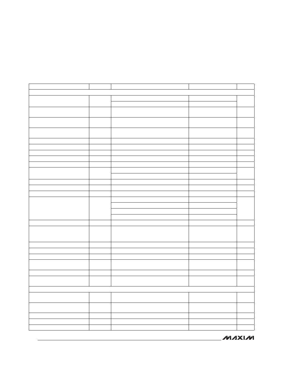
ELECTRICAL CHARACTERISTICS (continued)
(Typical Application Circuit, V+ = 2.7V to 5.0V, V
DD
= 1.7V to V+, T
A
= T
MIN
to T
MAX
, unless otherwise noted. Typical values are at
V+ = 3.3V, V
DD
= 2.5V, T
A
= +25NC.) (Note 4)
PARAMETER
SYMBOL
CONDITIONS
MIN
TYP
MAX
UNITS
BOOST CONVERTER
Undervoltage Lockout Threshold
V
UVLO
V+ rising
2.65
V
V+ falling
2.3
Undervoltage Lockout Threshold
Hysteresis
V
HYS
30
mV
Continuous Output Current
I
WLED
100% boost LED PWM, full-current setting,
R
B
= 6.67I, I
WLED
= V
FB
/R
B
30
mA
Operating Current
Run bit = 1, boost standby bit = 0, 0%
boost LED PWM
2
mA
LX Current Limit
V+ = 3.3V, T
A
= +25°C
430
500
570
mA
LX Saturation Voltage
I
LX
= 200mA
0.1
0.25
V
LX Leakage Current
I
LXOFF
0% boost LED PWM, V
LX
= 10V
8
F
A
OUT Leakage Current
I
OUTOFF
V
OUT
= 28V, boost converter in shutdown
16
23
F
A
Operating Frequency
f
BOOST
2
MHz
Minimum Duty Cycle
Continuous conduction mode
10
%
Discontinuous conduction mode
0
Maximum Duty Cycle
95
%
GM Amplifier Transconductance
250
F
S
FB Leakage Current
I
FB
V
FB
= 100mV
±0.01
Q
1
F
A
Feedback Output Voltage
V
FB
Half-current setting, V+ = 3.3V, T
A
= +25°C
94
100
106
mV
Full-current setting, V+ = 3.3V, T
A
= +25°C
190
200
210
Half-current setting
90
100
110
Full-current setting
175
200
225
Quick-Start Charge Current
I
QS
150
F
A
Quick-Start Time
From enable command STOP condition to
output regulation, C
COMP
= 0.047FF
(Note 7)
3.5
5
ms
Shutdown Discharge Resistance
R
COMP
20
kI
Output Current Line Regulation
3.0V < V+ < 5.0V
2
%/V
Thermal Shutdown Threshold
150
N
C
Thermal Shutdown Threshold
Hysteresis
9
N
C
Overvoltage Threshold
V
OV
V
OUT
Rising
28
29
30
V
Overvoltage Threshold
Hysteresis
V
OV_HYS
4
V
SERIAL INTERFACE (SDA, SCL, AD0, RST)
Input High Voltage
V
IH2
0.7 x
V
DD
V
Input Low Voltage
V
IL2
0.3 x
V
DD
V
Input Leakage Current
I
IN2
0.03
F
A
Output Low Voltage SDA
V
OL2
I
SINK
= 6mA
0.3
V
Input Capacitance
C
IN2
10
pF