Buck1 electrical characteristics, General electrical characteristics (continued) – Rainbow Electronics MAX8982X User Manual
Page 9
Power-Management ICs for
ICERA E400/E450 Platform
MAX8982A/MAX8982X
9
GENERAL ELECTRICAL CHARACTERISTICS (continued)
(MAX8982A: V
IN1A
= V
IN1B
= +5.0V and C
OUT1,2,3+CIN_
= 1000FF, MAX8982X: V
IN1A
= V
IN1B
= +3.3V and CO
UT1,2,3+CIN_
= 20FF,
C
REFBP
= 0.1FF, T
A
= -40NC to +85NC. Typical values are at T
A
= +25NC, unless otherwise noted.) (Note 3)
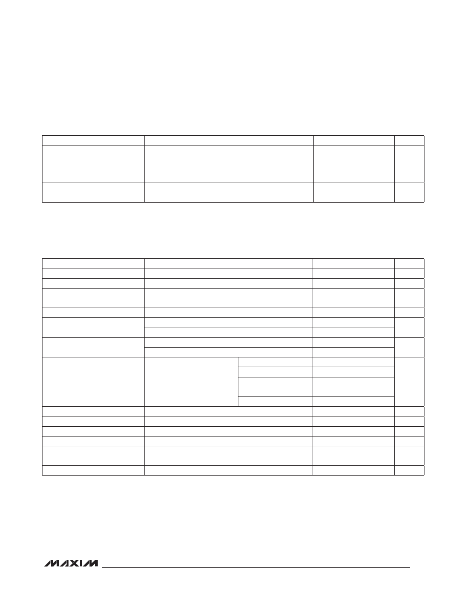
BUCK1 ELECTRICAL CHARACTERISTICS
(MAX8982A: V
IN1A
= V
IN1B
= +5.0V and C
OUT1,2,3+CIN_
= 1000µF, MAX8982X: V
IN1A
= V
IN1B
= +3.3V and C
OUT1,2,3+CIN_
= 20µF,
C
REFBP
= 0.1µF, C
OUT
= 10µF, L = 2.2µH, T
A
= -40NC to +85NC, unless otherwise noted. Typical values are at T
A
= +25NC.) (Note 3)
PARAMETER
CONDITIONS
MIN
TYP
MAX
UNITS
Maximum Pulse Width of Spikes
that Must be Suppressed by the
Input Filter of Both SDA and SCL
Signals
50
ns
Setup Time for STOP Condition
(t
SU_STO
)
0.6
F
s
PARAMETER
CONDITIONS
MIN
TYP
MAX
UNITS
Supply Current (Note 4)
No load, no switching
65
F
A
Default Output Voltage
I
LOAD
= 100mA
0.873
0.9
0.927
V
Output Voltage Accuracy
I
LOAD
= 100mA, V
BUCK1
tested at 0.6V, 0.775V, 1V,
1.2V in production (0.6V to 1.2V in 25mV steps)
-3
+3
%
Maximum Output Current
V
BUCK1
= 0.9V, T
A
= +25NC
1200
mA
Current Limit
pFET switch
1400
1800
2500
mA
nFET rectifier
1000
1400
1900
On-Resistance
pFET switch, I
LX1
= -150mA
0.3
I
nFET rectifier, I
LX1
= 150mA
0.15
Ramp-Up/Down Rate Control
Same for both up and down
RASD1[0:1] = 00
5
mV/
F
s
RASD1[0:1] = 01
10
RASD1[0:1] = 10
12.5
(default)
RASD1[0:1] = 11
25
Rectifier Off Current Threshold
40
mA
Minimum On-Time
t
ON
40
ns
Minimum Off-Time
t
OFF
40
ns
Efficiency (Note 4)
V
BUCK1
= 0.9V, I
LOAD
= 400mA
85
%
Shutdown Output Resistance
(Active Discharge Resistance)
I
2
C programmable, default OFF
1
kI
Output Load Regulation
Equal to inductor DC resistance divided by 4
R
L
/4
V/A