Pin description – Rainbow Electronics MAX8982X User Manual
Page 27
Power-Management ICs for
ICERA E400/E450 Platform
MAX8982A/MAX8982X
27
Pin Description
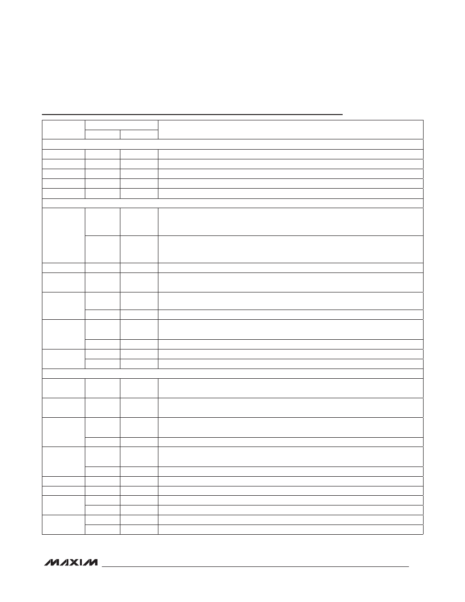
PIN
NAME
FUNCTION
MAX8982A MAX8982X
GROUND
A3
GND
GND
Analog Ground
F1
PGND1
PGND1
Power Ground for BUCK1
E1
PGND2
PGND2
Power Ground for BUCK2
E7
PGND3
PGND3
Power Ground for BUCK3
F6, F7
PGND4
PGND4
Power Ground for BUCK4
INPUT SUPPLY
F4
IN1A
—
Input Supply to the IC. The operating voltage range for the MAX8982A is 4.1V to 5.5V.
Connect three 330FF tantalum capacitors as close as possible to IN1A and IN1B.
Connect IN1A to IN1B.
—
IN1A
Input Supply to the IC. The operating voltage range for the MAX8982X is 2.9V to 5.5V.
Bypass with a 22FF ceramic capacitor as close as possible to IN1A and IN1B. Connect
IN1A to IN1B.
E4
IN1B
IN1B
Input Supply to the IC. Connect IN1B to IN1A.
C1
IN3
IN3
Input Supply for LDO4 and LDO9. Connect IN3 to the BUCK2 output. Bypass IN3 with a
2.2FF ceramic capacitor as close as possible to IN3.
F3
IN4
—
Input Supply for LDO8. Bypass with a 1FF ceramic capacitor as close as possible to IN4.
The IN4 operating range is from 3.0V to 5.5V. Connect IN4 to either IN1A and IN1B.
—
IN4
Connect IN4 to Both IN1A and IN1B
B7
V
DDA
—
Power Input for LDO1 and LDO2. Connect V
DDA
to V
DDB
. Bypass V
DDA
with a 10FF
ceramic capacitor as close as possible to V
DDA
.
—
V
DDA
Power Input for LDO1 and LDO2. Connect V
DDA
to V
DDB
, IN1A, and IN1B.
B6
V
DDB
—
Power Input for LDO3, LDO5, LDO6, and LDO7. Connect V
DDB
to V
DDA
.
—
V
DDB
Power Input for LDO3, LDO5, LDO6, and LDO7. Connect V
DDB
to V
DDA,
IN1A, and IN1B
.
BUCK CONVERTERS
F2
LX1
LX1
BUCK1 Inductor Connection. LX1 connects to the drains of the internal p-channel and
n-channel MOSFETs.
D1
LX2
LX2
BUCK2 Inductor Connection. LX2 connects to the drains of the internal p-channel and
n-channel MOSFETs.
D7
LX3
—
BUCK3 Inductor Connection. LX3 connects to the drains of the internal p-channel and
n-channel MOSFETs.
—
DNC
Do Not Connect
E5, F5
LX4
—
BUCK4 Inductor Connection. LX4 connects to the drains of the internal p-channel and
n-channel MOSFETs. Connect the two LX4 bumps together externally.
—
DNC
Do Not Connect
E2
BUCK1
BUCK1
BUCK1 Output Feedback
D2
BUCK2
BUCK2
BUCK2 Output Feedback
D6
BUCK3
—
BUCK3 Output Feedback
—
DNC
Do Not Connect
E6
BUCK4
—
BUCK4 Output Feedback
—
DNC
Do Not Connect