Figure 16. i2c timing diagram, Figure 17. writing to the ics, Slave address – Rainbow Electronics MAX8982X User Manual
Page 42: Write operations, Slave address write operations, Figure 16. i, C timing diagram
Power-Management ICs for
ICERA E400/E450 Platform
MAX8982A/MAX8982X
42
Slave Address
The ICs act as a slave transmitter/receiver. The slave
address of the ICs is:
10000010 (0x82) for write operations
10000011 (0x83) for read operations
The least significant bit is the read/write indicator.
1
0
0
0
0
0
1
R/W
Write Operations
Use the following procedure to write to a sequential
block of registers (Figure 17):
1) The master sends a start command.
2) The master sends the 7-bit slave address followed
by a write bit (0x82).
3) The addressed slave asserts an acknowledge by
pulling SDA low.
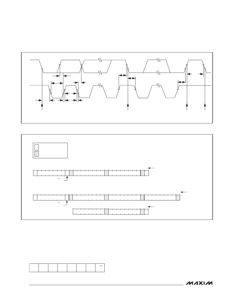
Figure 16. I
2
C Timing Diagram
Figure 17. Writing to the ICs
SCL
SDA
t
R
t
F
t
BUF
START
CONDITION
STOP
CONDITION
REPEATED START CONDITION
START CONDITION
t
SU_STO
t
HD_STA
t
SU_STA
t
HD_DAT
t
SU_DAT
t
LOW
t
HIGH
t
HD_STA
1
S
NUMBER OF BITS
R/W
SLAVE ADDRESS
7
0
1
8
REGISTER POINTER
1
1
SLAVE TO
MASTER
MASTER TO
SLAVE
LEGEND
a) WRITING TO A SINGLE REGISTER WITH THE WRITE BYTE PROTOCOL
1
S
NUMBER OF BITS
R/W
SLAVE ADDRESS
7
0
1
8
REGISTER POINTER X
1
A
1
8
DATA X
1
b) WRITING TO MULTIPLE REGISTERS
...
8
DATA X+n-1
1
NUMBER OF BITS
...
8
DATA X+1
1
A
A
A
A
A
A
8
DATA
1
P
1
A
8
DATA X+n
1
A P