Rainbow Electronics MAX8982X User Manual
Page 64
Power-Management ICs for
ICERA E400/E450 Platform
MAX8982A/MAX8982X
64
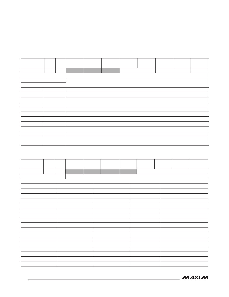
Table 51. On/Off Register (On/Off Control for BUCK3, BUCK4, and the Internal 32kHz Clock)
Table 52. BUCK3 Register (Output Voltage Setting for BUCK3)
Note: The BUCK3 and BUCK4 bits are not used by the MAX8982X.
Note: This register is not used by the MAX8982X.
ADDRESS
(HEX)
POR
(HEX)
R/W
BIT 7
BIT 6
BIT 5
BIT 4
BIT 3
BIT 2
BIT 1
BIT 0
70
03
R/W
Reserved
Reserved
Reserved
BUCK4[1:0]
BUCK3[1:0]
32KCLK
BITS 7:5
Reserved, write 000 to these bits.
NAME
DESCRIPTION
BUCK4[1]
BUCK4[0]
0
0
BUCK4 off (in I
2
C on mode).
0
1
BUCK4 on (in I
2
C on mode).
1
0
BUCK4 on (in PWR_REQ on mode) (Group B).
1
1
BUCK4 on (in PWR_REQ on mode) (Group B).
BUCK3[1]
BUCK3[0]
DESCRIPTION
0
0
BUCK3 OFF (in I
2
C on mode).
0
1
BUCK3 ON (in I
2
C on mode).
1
0
BUCK3 ON (in PWR_REQ on mode).
1
1
BUCK3 ON (in PWR_REQ on mode).
NAME
POR
DESCRIPTION
32KCLK
1
1: Turn on 32kHz.
0: Turn off 32kHz.
ADDRESS
(HEX)
POR
(HEX)
R/W
BIT 7
BIT 6
BIT 5
BIT 4
BIT 3
BIT 2
BIT 1
BIT 0
72
06
R/W
Reserved
Reserved
Reserved
Reserved
SD3[3:0]
BITS 7:4
Reserved, write 0000 to these bits.
DESCRIPTION
BIT 3
BIT 2
BIT 1
BIT 0
V
PROG
(V)
0
0
0
0
2.90
0
0
0
1
2.95
0
0
1
0
3.00
0
0
1
1
3.05
0
1
0
0
3.10
0
1
0
1
3.15
0
1
1
0
3.20
0
1
1
1
3.25
1
0
0
0
3.30
1
0
0
1
3.35
1
0
1
0
3.40
1
0
1
1
3.45
1
1
0
0
3.50
1
1
0
1
3.55
1
1
1
0
3.60
1
1
1
1
3.65