Figure 7. dvs1 logic diagram, Truth table, Buck1, buck2, and buck3 step-down converters – Rainbow Electronics MAX8982X User Manual
Page 37: Setting the output voltage on buck1, Dynamic voltage scaling (dvs) function on buck 1
Power-Management ICs for
ICERA E400/E450 Platform
MAX8982A/MAX8982X
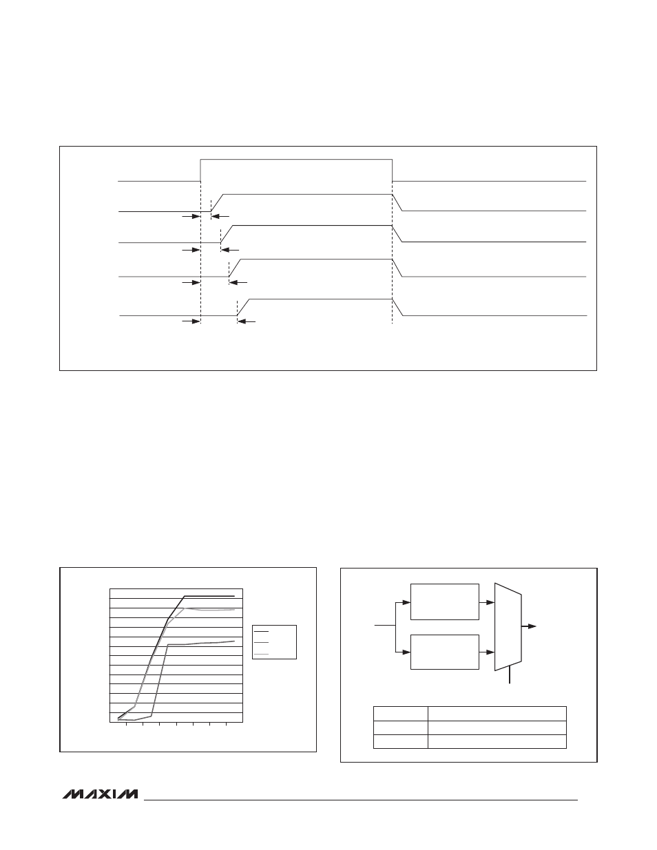
37
BUCK1, BUCK2, and BUCK3
Step-Down Converters
The step-down converters are optimized for high effi-
ciency over a wide load range, small external component
size, low output ripple, and excellent transient response.
The step-down converters also feature an internal
MOSFET switch with optimized on-resistance and an
internal synchronous rectifier to maximize the efficiency
and reduce the number of external components. The ICs
use a proprietary hysteretic PWM control scheme that
switches with a nearly fixed frequency. Figure 6 shows
the frequency variation versus load current with a 5V
input supply and at T
A
= +25°C.
Setting the Output Voltage on BUCK1
The default output is 0.9V. The BUCK1 voltage is program-
mable through I
2
C from 0.6V to 1.2V in 25mV increments.
Dynamic Voltage Scaling (DVS)
Function on Buck 1
BUCK1 includes DVS that allows two output voltages
to be programmed through I
2
C, and an external con-
trol input to select between the two voltages. Toggling
DVS1 changes the BUCK1 output voltage on-the-fly
between the two programmed voltages (Figure 7). Each
BUCK1DVS_ register specifies a voltage in the 0.6V to
1.2V range in 25mV increments.
Figure 5. MAX8982A/MAX8982X Power-On Timing Diagram in PWR_REQ ON Mode After Power-Up
Figure 6. Frequency Variation vs. Load Current with a 5V Input
Supply
Figure 7. DVS1 Logic Diagram
DVS1
I
2
C INTERFACE
0.6V TO 1.2V
IN 25mV STEPS
BUCK1DVS1
(0X3F)
(DEFAULT = 0.9V)
BUCK1DVS2
(0X40)
(DEFAULT = 0.9V)
BUCK1 OUTPUT
(DEFAULT = 0.9V)
~10µs
100µs
200µs
375µs
PWR_REQ
GROUP A : OUT 2,*
GROUP B : LDO1,*
BUCK 2, BUCK 3**
OUT 3, BUCK 4**
GROUP C : OUT6,*
OUT5, OUT7, OUT8**
GROUP D : BUCK 1*, OUT4,*
OUT9
OUTPUT DECAY DEPENDS ON THE LOAD
(BUILT-IN TIME DELAY TO
ENABLE REGULATORS)
*THESE REGULATORS DEFAULT TO PWR_REQ CONTROL. THE OTHERS MUST BE PROGRAMED TO PWR_REQ CONTROL BY I
2
C.
**BUCK3, BUCK4, AND OUT8 ARE FOR THE MAX8982A ONLY.
FREQUENCY vs. LOAD AT 5V INPUT
LOAD (mA)
FREQUENCY (MHz)
0.2
0.4
0.6
0.8
1.0
1.2
1.4
1.6
1.8
2.0
2.2
2.4
2.6
2.8
0
1
10
50
100 200 300 400 500
BUCK1
BUCK2
BUCK3
DVS1
BUCK1 OUTPUT
High
Set by BUCK1DVS2 register
Low
Set by BUCK1DVS1 register
TRUTH TABLE