Table 3. external component list for figure 2, Detailed description, Power-on/off control – Rainbow Electronics MAX8982X User Manual
Page 34: Pwr_req
Power-Management ICs for
ICERA E400/E450 Platform
MAX8982A/MAX8982X
34
Detailed Description
Power-On/Off Control
The power-on/off state diagram is shown in Figure 3.
When the IN1_ supply voltage is valid and EN is high,
the default power supplies turn on in sequence (Figure
4). Once powered up, any step-down or LDO output can
be enabled or disabled through I
2
C, or they can be pro-
grammed to be controlled by the PWR_REQ logic input.
PWR_REQ
PWR_REQ is a control input from baseband chipset used
to enable/disable specified regulators.
After power-up, when PWR_REQ goes logic-high, any
step-down or LDO output programmed for PWR_REQ
control is enabled in a predefined sequence. The regulators
are powered up in four groups as shown in Figure 5. See the
following for the regulators belonging to each group. When
PWR_REQ goes logic-low, all regulators programmed for
PWR_REQ control are turned off simultaneously.
Any regulator that is set to on or off though I
2
C is not
affected by PWR_REQ, except for BUCK1. The pro-
grammed values in BUCK1DVS1 and BUCK1DVS2 are
reset to their defaults when PWR_REQ goes low even in
normal operation.
Group A: BUCK3 (MAX8982A only)
LDO2 (default is PWR_REQ On mode)
BUCK2
Group B: LDO1 (default is PWR_REQ On mode)
LDO3
BUCK4 (MAX8982A only)
Group C: LDO6 (default is PWR_REQ On mode)
LDO5
LDO7
LDO8 (MAX8982A only)
Group D: BUCK1 (default is PWR_REQ On mode)
LDO4 (default is PWR_REQ On mode)
LDO9
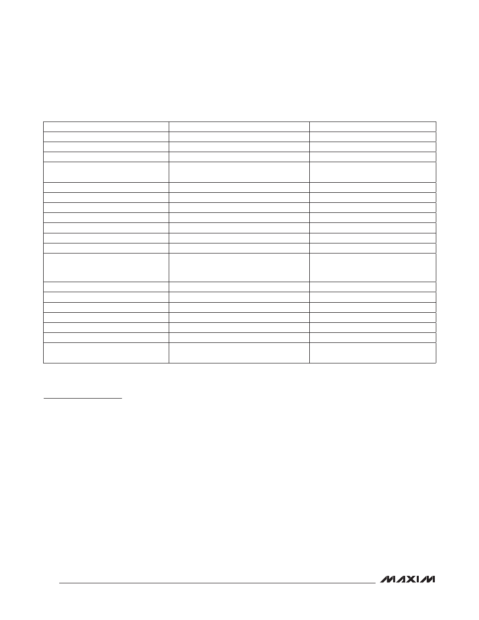
Table 3. External Component List for Figure 2
Note: Input/output capacitance should be as close as possible to the IC. All capacitors are ceramic X5R or X7R, unless otherwise noted.
LOCATION
EXTERNAL COMPONENTS
NOTES
IN1A, IN1B
22FF
Buck stability
IN3
2.2FF
Input for LDO4 and LDO9
IN4
Connect to IN1A and IN1B
OUT1
4.7FF
LDO compensation and load transient
response
OUT2
1.0FF
LDO compensation
OUT3
1.0FF
LDO compensation
OUT4
2.2FF
LDO compensation
OUT5
1.0FF
LDO compensation
OUT6
1.0FF
LDO compensation
VSIM (OUT7)
1.0FF
LDO compensation
OUT9
2.2FF
LDO compensation
V
DDA
, V
DDB
Total capacitance R total output capacitance
for LDO1, LDO2, LDO3, LDO5, LDO6, and
VSIM.
All LDOs stability. Connect V
DDA
and
V
DDB
to IN1A and IN1B.
BUCK1 for BB Core
2.2FF
For low noise, 1.2A continuous load
BUCK2 for BB System IO
2.2FF
For low noise
LX1
1FH to 4.7FH
2.2FH recommended (Table 60)
LX2
1FH to 4.7FH
1.0FH recommended (Table 60)
REFBP
0.1FF
Noise filter
EN
A pulldown resistor, if necessary
Any Bump Required to Pass 8kV
Module Level ESD
0.1FF
Absorb ESD energy