Figure 8. buck1 ramp-up/down slope control, Table 4. buck1 ramp-up/down slope control settings, Ramp-up/down slope control on buck1 – Rainbow Electronics MAX8982X User Manual
Page 38: Setting the output voltage on buck2, Setting the output voltage on buck3, Buck4 step-down converter for pa (power amplifier), Setting the output voltage on buck4, Linear regulators, Reference bypass (refbp), Thermal overload protection
Power-Management ICs for
ICERA E400/E450 Platform
MAX8982A/MAX8982X
38
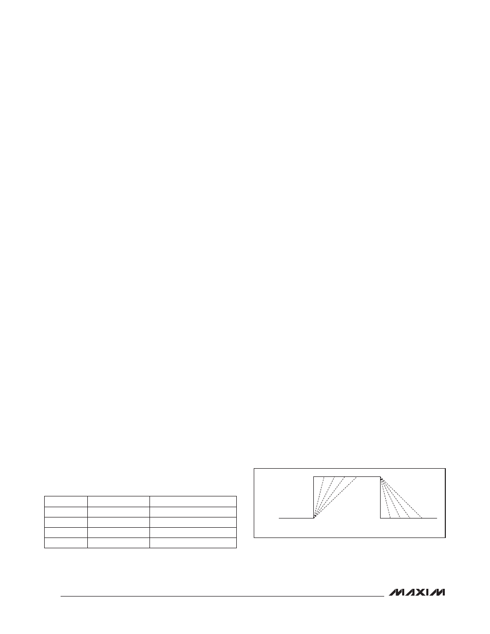
Ramp-Up/Down Slope Control on BUCK1
BUCK1 uses a controlled ramp rate when it is enabled
and when changing between output voltage settings.
Four programmable slew rates are available for BUCK1.
The default value is 12.5mV/Fs (Table 4). The same slew
rate is applied for ramp-up/down.
Setting the Output Voltage on BUCK2
The BUCK2 output voltage is fixed at 1.8V. No program-
mable output is available.
Setting the Output Voltage on BUCK3
The BUCK3 default output is 3.2V. The BUCK3 output
voltage is programmable from 2.9V to 3.65V in 50mV
increments through I
2
C. BUCK3 is only available on the
MAX8982A.
BUCK4 Step-Down Converter
for PA (Power Amplifier)
BUCK4 is a 2MHz fixed-frequency PWM step-down
converter, typically used to supply the power amplifier
(PA). The BUCK4 load capability is 1.8A. BUCK4 is only
available on the MAX8982A.
Setting the Output Voltage on BUCK4
The default output voltage is 3.4V. The BUCK4 output
voltage is programmable between 3.0V and 3.75V in
50mV increments through I
2
C.
Linear Regulators
All linear regulators are designed for low-drop, low noise,
high PSRR, and low quiescent current to minimize power
consumption. If the input voltage is above UVLO thresh-
old and power-on is logic-high, the default linear regula-
tor (LDO3) turns on. The other LDOs are turned on and
off by the baseband processor through the I
2
C interface
or PWR_REQ control signal. All LDO output voltages are
programmable through the I
2
C interface within option
voltages.
Reference Bypass (REFBP)
The reference bypass is for low noise filtering only and
must not be loaded. Bypass REFBP with a 0.1FF ceramic
capacitor. The REFBP voltage is 0.8V (typ). Do not use
REFBP to provide power to external circuitry.
Thermal Overload Protection
If the internal die temperature of any LDOs or step-
down regulators reaches +160NC, the ICs shut down the
regulator locally. The regulator is reenabled after it cools
by 10NC. The ICs also contain a single +125NC thermal
detector located in the center of the die. When the tem-
perature at the center of the die exceeds +125NC, this
detector triggers and activates an interrupt.
Undervoltage Lockout (UVLO)
The ICs monitor the voltage at the IN1_ power input.
When this voltage drops below 3.5V (MAX8982A) or
2.4V (MAX8982X), the ICs shut down. The ICs turn on
when this voltage rises above 3.8V (MAX8982A) or 2.7V
(MAX8982X) and EN is high. After a UVLO event, all reg-
isters are reset to their POR value.
Overvoltage Protection (OVP)
If the voltage on the IN1_ or IN4 inputs exceeds 5.75V
(typ), the ICs shut down. When the supply voltage
returns to within the valid operating range and EN is
high, the ICs turn on and go through a normal power-up
sequence. All registers are reset to their default power-
on reset (POR) value.
Power-On Reset (POR)
Power-on reset (POR) for I
2
C occurs when the ICs turn
off due to UVLO, OVP, or EN = low. This condition puts
the IC into shutdown and then clears all previously pro-
grammed output voltages in the internal registers.
The programmed values in BUCK1DVS1 and
BUCK1DVS2 are also reset to their defaults when
PWR_REQ goes low in normal operation mode.
Figure 8. BUCK1 Ramp-Up/Down Slope Control
Table 4. BUCK1 Ramp-Up/Down Slope
Control Settings
V
BUCK1
UP SLOPE
CONTROL
DOWN
SLOPE
CONTROL
RASD1[1]
RASD1[0]
SLEW RATE (mV/µs)
0
0
5
0
1
10
1
0
12.5 (default)
1
1
25