Applications information, Chip information – Rainbow Electronics MAX9486 User Manual
Page 7
SHDN
Mode
The MAX9486 features a shutdown mode with a supply
current less than 8µA (typ). Drive SHDN low to get the
device into shutdown mode. In this mode, all the out-
puts go low and both PLLs are powered down. After
SHDN goes high, the outputs still stay low for an addi-
tional 256ms to allow both PLLs to be stabilized before
the outputs are enabled again.
Applications Information
Crystal Selection
The MAX9486 uses a 17.664MHz crystal as the base
frequency for the VCXO. It is important to use a correct
type of quartz crystal to avoid reducing frequency
pulling range, or excessive output phase jitter.
Choose an AT-cut crystal that oscillates at 17.664MHz
on its fundamental mode with a variation of
±25ppm
including frequency accuracy and operating tempera-
ture range. The crystal’s load capacitance should be
14pF. Pulling range may vary depending on the crystal
used. Refer to the MAX9486 evaluation kit for details.
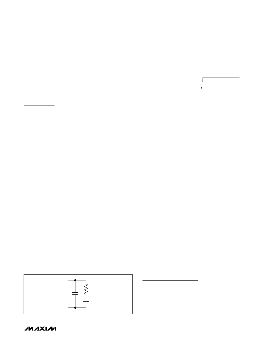
PLL1 Loop Filter
The MAX9486 features two PLLs: PLL1 and PLL2. The
first phased-lock loop, PLL1, contains an integrated
VCXO that uses an external crystal to track the input
reference signal and attenuate input jitter. Figure 1
shows the external loop filter of the PLL containing
resistor R1 and two capacitors, C1 and C2. This loop
filter is connected between LP1 and LP2 as shown in
the Typical Operating Circuit. The loop-filter bandwidth
is determined by C1, C2, R1, and R
SET
where R
SET
is
used to set the value of the charge-pump current. The
typical values of C1, C2, R1, and R
SET
are 22nF,
560pF, 1000k
Ω, and 13kΩ, respectively.
Use the following equation to calculate a PLL loop
bandwidth in Hz:
BW = (R1 x I
SETI
x 940) / N
where R1 (
Ω) is the resistor in the PLL1 loop filter
(Figure 1), I
SETI
(A) is the charge-pump current calcu-
lated from the equation in the Charge-Pump Current
Setting section, and N is the crystal PLL frequency
divider equal to 2208.
The loop-damping factor is calculated by:
where C1 (F) and R1 (
Ω) are the values of the capacitor
and the resistor in the PLL1 loop filter shown in
Figure 1; I
SETI
is calculated as shown in the Charge-
Pump Current Setting section and N = 2208.
The following equation shows the relationship between
components C1 and C2 in the loop filter:
C2
≤ C1/20
Charge-Pump Current Setting
The MAX9486 also allows external setting of the charge-
pump current in PLL1. Connect a resistor from SETI to
GNDP to set the PLL1 charge-pump current:
Charge-Pump Current = 2.4 x 1000 / (R
SET
(k
Ω) + 1)
where R
SET
is in k
Ω and the value of the charge-pump
current is in µA.
The loop response can be adjusted to meet individual
application requirements since the charge-pump cur-
rent and all the filter components for the VCXO loop
can be set externally.
Board Layout and Bypassing
The MAX9486’s high-oscillator frequency makes proper
layout important to ensure stability. For best performance,
place components as close as possible to the device.
Digital or AC transient signals on GND can create noise
at the clock outputs. Return GND to the highest quality
ground available. Bypass V
DD
and V
DDP
with 0.1µF
and 0.001µF capacitors, placed as close to the device
as possible. Careful PC board ground layout minimizes
crosstalk between the outputs and digital inputs.
Traces must be as short as possible on LP1 and LP2
and connect the capacitors and the resistor as close as
possible to the device.
Chip Information
TRANSISTOR COUNT: 7512
PROCESS: CMOS
DampingFactor
R
I
C
N
SETI
=
Ч
Ч
Ч
1
1
2
5900
MAX9486
8kHz Reference Clock Synthesizer
with Multiple Outputs at 35.328MHz
_______________________________________________________________________________________
7
R1
C1
C2
LP1
LP2
Figure 1. Typical Loop Filter